ADCMP582
ADCMP582 is Ultrafast SiGe Voltage Comparators manufactured by Analog Devices.
- Part of the ADCMP580 comparator family.
- Part of the ADCMP580 comparator family.
FEATURES
180 ps propagation delay 25 ps overdrive and slew rate dispersion 8 GHz equivalent input rise time bandwidth 100 ps minimum pulse width 37 ps typical output rise/fall 10 ps deterministic jitter (DJ) 200 fs random jitter (RJ)
- 2 V to +3 V input range with +5 V/- 5 V supplies On-chip terminations at both input pins Resistor-programmable hysteresis Differential latch control Power supply rejection > 70 d B
APPLICATIONS
Automatic test equipment (ATE) High speed instrumentation Pulse spectroscopy Medical imaging and diagnostics High speed line receivers Threshold detection Peak and zero-crossing detectors High speed trigger circuitry Clock and data signal restoration
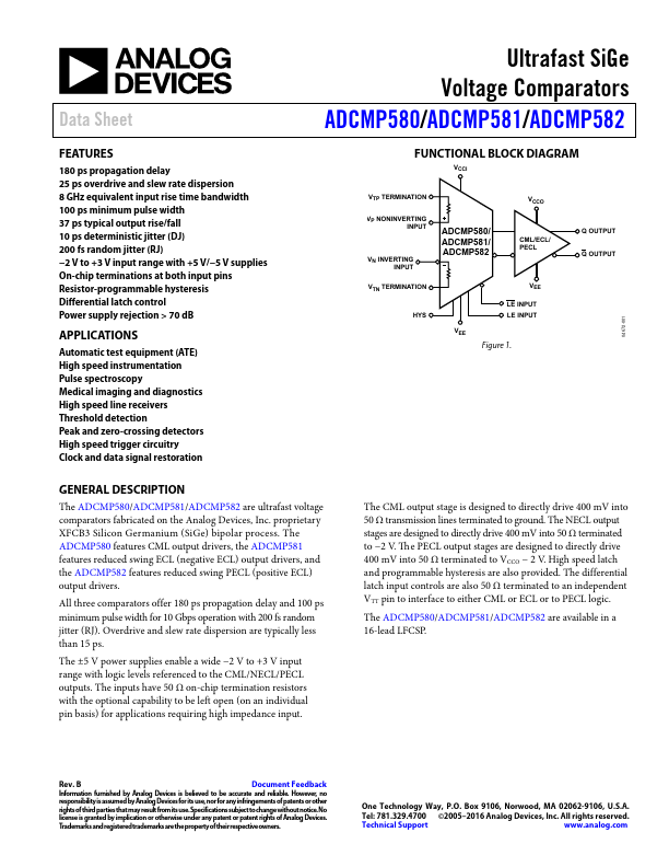
FUNCTIONAL BLOCK DIAGRAM
VCCI
VTP TERMINATION VP NONINVERTING
INPUT
VN INVERTING INPUT
VTN TERMINATION HYS
ADCMP580/ ADCMP581/ ADCMP582
VCCO
CML/ECL/ PECL
LE INPUT LE INPUT VEE
Figure 1.
Q OUTPUT Q OUTPUT
04672-001
GENERAL DESCRIPTION
The ADCMP580/ADCMP581/ADCMP582 are ultrafast voltage parators fabricated on the Analog Devices, Inc. proprietary XFCB3 Silicon Germanium (Si Ge) bipolar process. The ADCMP580 features
CML output drivers, the ADCMP581 features reduced swing ECL (negative ECL) output drivers, and the ADCMP582 features reduced swing PECL (positive ECL) output drivers.
All three parators offer 180 ps propagation delay and 100 ps minimum pulse width for 10 Gbps operation with 200 fs random jitter (RJ). Overdrive and slew rate dispersion are typically less than 15 ps.
The ±5 V power supplies enable a wide
- 2 V to +3 V input range with logic levels referenced to the CML/NECL/PECL outputs. The inputs have 50 Ω on-chip termination resistors with the optional capability to be left open (on an individual pin basis) for applications requiring high impedance input.
The CML output stage is designed to directly drive 400 m V into 50 Ω transmission lines terminated to ground. The NECL output stages are designed to directly drive 400 m V into 50 Ω terminated to
- 2 V. The PECL output stages are...