Datasheet Summary
a
Features
Two Mask Programmable Sets of Five Reference Levels Dual 10-Bit DACs for Flicker Offset and Range Adjustment Integrated V Switching Single-Supply Operation: 5.0 V Low Supply Current: 300 A Global Power Save Mode: 1 A Max Fast Settling Time for Load Change: 20 s Stable with 20 nF/100 ⍀ Loads CMOS/TTL Input Levels APPLICATIONS Color TFT Cell Phones Color TFT PDAs
VL VDD VDD/2 VREF+ 10-BIT DAC A VREF-
Integrated LCD Grayscale Generator ADD8502
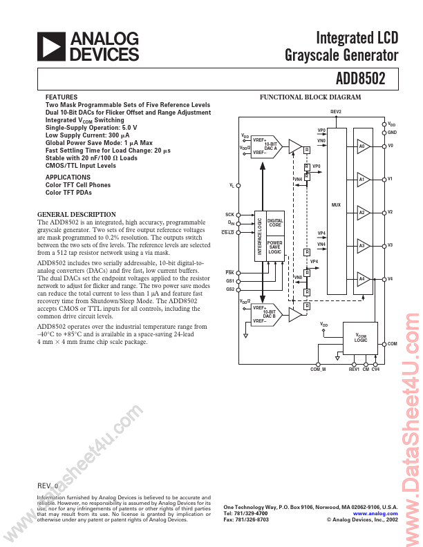
FUNCTIONAL BLOCK DIAGRAM
REV2 VDD VP0 VN0 R A0 V0 GND
R VN4 R
VP0 A1 V1
GENERAL DESCRIPTION
INTERFACE LOGIC
A2 DIGITAL CORE VP4 POWER SAVE LOGIC VN4 R VP4 A3
V2
The ADD8502 is an integrated, high accuracy,...