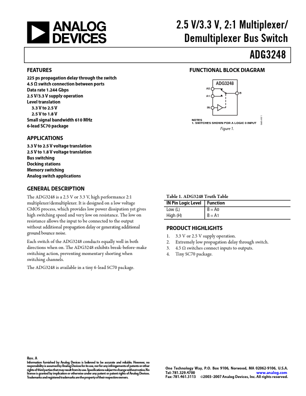
Datasheet4U Logo Datasheet4U.com

ADG3248 - Multiplexer / Demultiplexer Bus Switch

General Description

The ADG3248 is a 2.5 V or 3.3 V, high performance 2:1 multiplexer/demultiplexer.

It is designed on a low voltage CMOS process, which provides low power dissipation yet gives high switching speed and very low on resistance.

Key Features

  • 225 ps propagation delay through the switch 4.5 Ω switch connection between ports Data rate 1.244 Gbps 2.5 V/3.3 V supply operation Level translation 3.3 V to 2.5 V 2.5 V to 1.8 V Small signal bandwidth 610 MHz 6-lead SC70 package.

📥 Download Datasheet

Full PDF Text Transcription for ADG3248 (Reference)

Note: Below is a high-fidelity text extraction (approx. 800 characters) for ADG3248. For precise diagrams, and layout, please refer to the original PDF.

FEATURES 225 ps propagation delay through the switch 4.5 Ω switch connection between ports Data rate 1.244 Gbps 2.5 V/3.3 V supply operation Level translation 3.3 V to 2....

View more extracted text
1.244 Gbps 2.5 V/3.3 V supply operation Level translation 3.3 V to 2.5 V 2.5 V to 1.8 V Small signal bandwidth 610 MHz 6-lead SC70 package APPLICATIONS 3.3 V to 2.5 V voltage translation 2.5 V to 1.8 V voltage translation Bus switching Docking stations Memory switching Analog switch applications GENERAL DESCRIPTION The ADG3248 is a 2.5 V or 3.3 V, high performance 2:1 multiplexer/demultiplexer. It is designed on a low voltage CMOS process, which provides low power dissipation yet gives high switching speed and very low on resistance. The low on resistance allows the input to be connected to the output without additional p