Analog Devices ADG5207
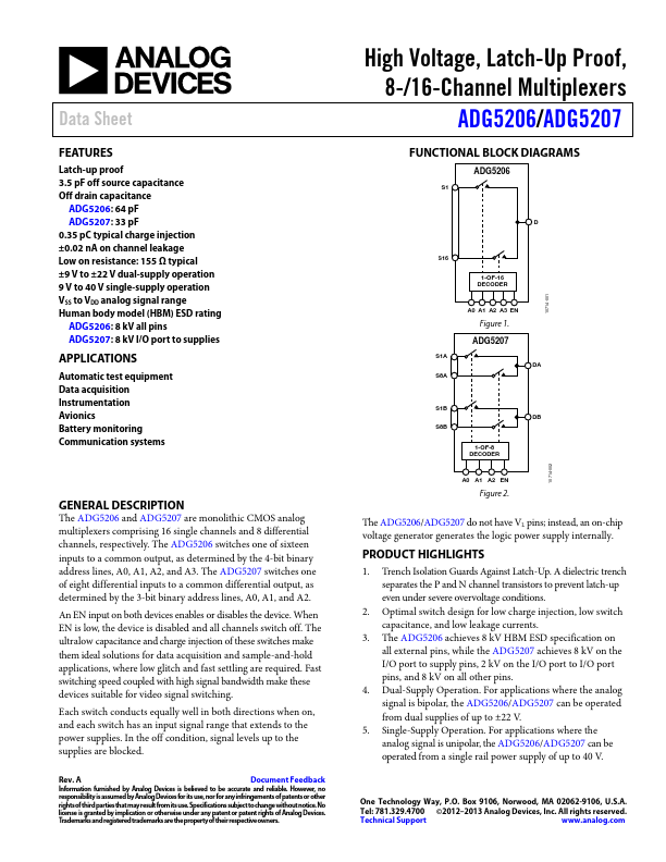
The ADG5207 switches one of eight differential inputs to a common differential output, as determined by the 3-bit binary address lines, A0, A1, and A2. When EN is low, the device is disabled and all channels switch off. The ultralow capacitance and charge injection of these switches make them ideal solutions for data acquisition and sample-and-hold applications, where low glitch and fast settling are required.
| Part No. |
ADG5207 |
| Datasheet |
ADG5207
Download
|
| Manufacturer |
 Analog Devices |
| Description |
8-/16-Channel Multiplexers |
| Buy |
Stock & Price
|
FEATURES
Latch-up proof 3.5 pF off source capacitance Off drain capacitance ADG5206: 64 pF ADG5207: 33 pF 0.35 pC typical charge injection ±0.02 nA on channel leakage Low on resistance: 155 Ω typical ±9 V to ±22 V dual-supply operation 9 V to 40 V single-supply operation VSS to VDD analog signal range Human body model (HBM) ESD rating ADG5206: 8 kV all pins ADG5207: 8 kV I/O port to supplies APPLICATIONS
Automatic test equipment Data acquisition Instrumentation Avionics Battery monitoring Communication systems GENERAL DESCRIPTION
The ADG5206 and ADG5207 are monolithic CMOS analog multiplexers comprising 16 single channels and 8 differential channels, respectively. The ADG5206 switches one of sixteen inputs to a common output, as determined by the 4-bit binary address lines, A0, A1, A2, and A3. An EN input on both devices enables or disables the device. Fast switching speed coupled with high signal bandwidth make these devices suitable for video signal switching. Each switch conducts equally well in both directions when on, and each switch has an input signal range that extends to the power supplies.