Analog Devices ADG613
Quad SPST Switches
| Part No. | ADG613 |
|---|---|
| Datasheet | ADG613 Download |
| Manufacturer |  Analog Devices |
| Description | Quad SPST Switches |
| Buy | Stock & Price |
FEATURES
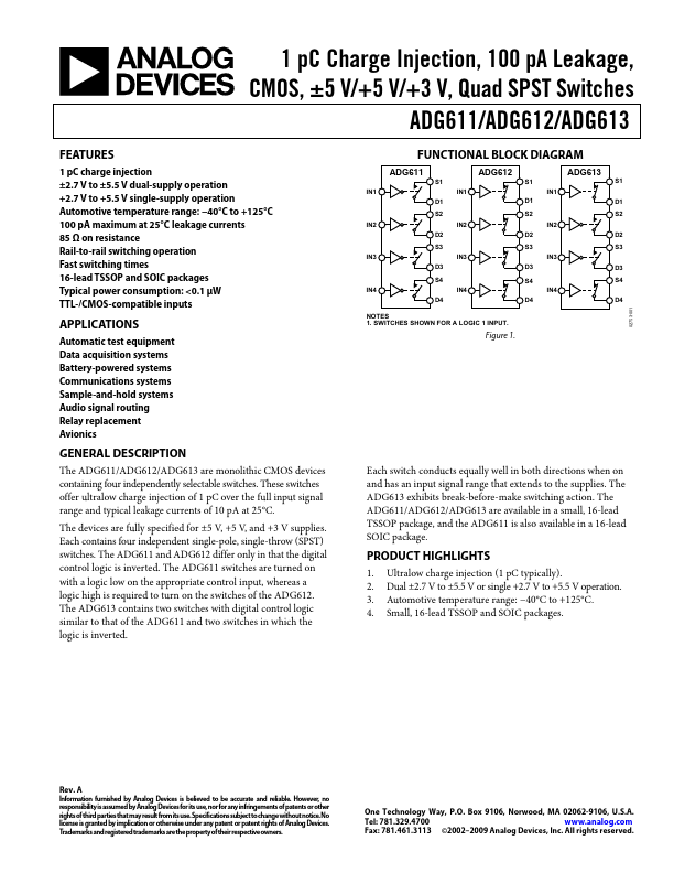
1 pC charge injection ±2.7 V to ±5.5 V dual-supply operation +2.7 V to +5.5 V single-supply operation Automotive temperature range: −40°C to +125°C 100 pA maximum at 25°C leakage currents 85 Ω on resistance Rail-to-rail switching operation Fast switching times 16-lead TSSOP and SOIC packages Typical power consumption: <0.1 μW TTL-/CMOS-compatible inputsAPPLICATIONS
Automatic test equipment Data acquisition systems Battery-powered systems Communications systems Sample-and-hold systems Audio signal routing Relay replacement AvionicsGENERAL DESCRIPTION
The ADG611/ADG612/ADG613 are monolithic CMOS devices containing four independently selectable switches. These switches offer ultralow charge injection of 1 pC over the full input signal range and typical leakage currents of 10 pA at 25°C. The devices are fully specified for ±5 V, +5 V, and +3 V supplies. Each contains four independent single-pole, single-throw (SPST) switches. The ADG611 and ADG612 differ only in that the digital control logic is inverted.