ADG836
ADG836 is 0.5CMOS 1.65 V TO 3.6 V Dual SPDT/2:1 MUX manufactured by Analog Devices.
- Part of the ADG comparator family.
- Part of the ADG comparator family.
0.5 CMOS 1.65 V TO 3.6 V Dual SPDT/2:1 MUX ADG836
Features
0.5 Typical On Resistance 0.8 Maximum On Resistance at 125°C 1.65 V to 3.6 V Operation Automotive Temperature Range:
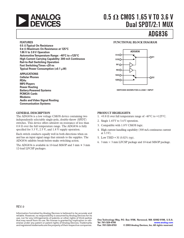
- 40°C to +125°C High Current Carrying Capability: 300 mA Continuous Rail-to-Rail Switching Operation Fast Switching Times <20 ns Typical Power Consumption (<0.1 W) APPLICATIONS Cellular Phones PDAs MP3 Players Power Routing Battery-Powered Systems PCMCIA Cards Modems Audio and Video Signal Routing munication Systems GENERAL DESCRIPTION FUNCTIONAL BLOCK DIAGRAM
- -
- -
- -
- -
- -
- -
- -
- -
- -
- -
- -
- -
- -
- -
- -
- -
- -
- -
- -
- -
- -
- -
- -
- -
- -
-...