Analog Devices ADL5331
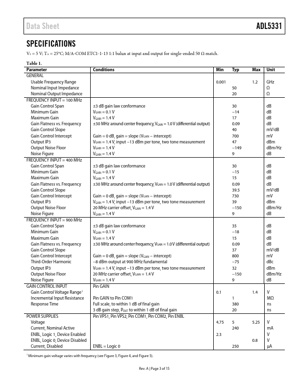
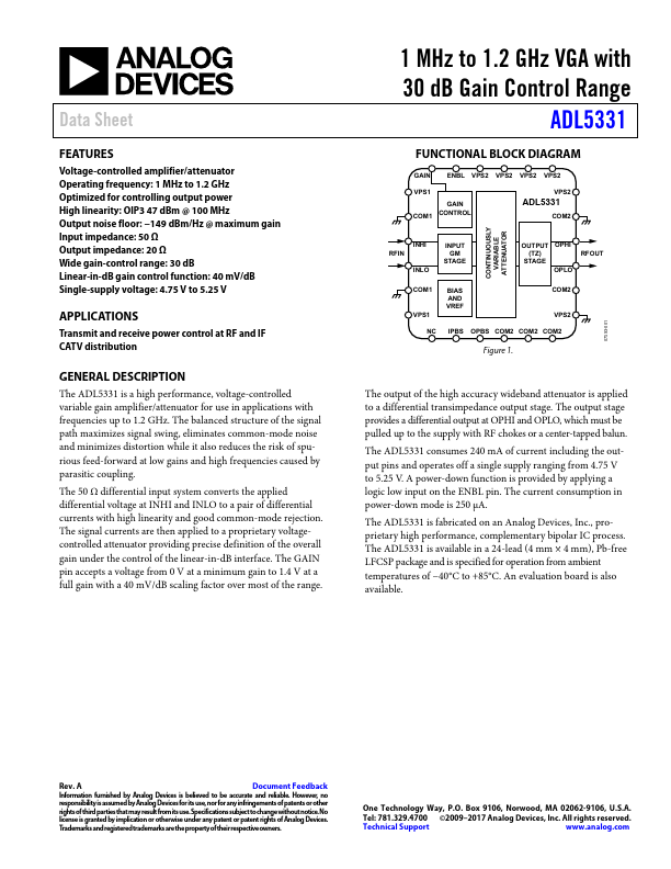
The ADL5331 is a high performance, voltage-controlled variable gain amplifier/attenuator for use in applications with frequencies up to 1.2 GHz. The balanced structure of the signal path maximizes signal swing, eliminates common-mode noise and minimizes distortion while it also reduces the risk of spurious feed-forward at low gains and high frequencies caused by parasitic coupling. The 50 Ω differential input system converts the applied differential voltage at INHI and INLO to a pair of differential currents with high linearity and good common-mode rejection.| Part No. | ADL5331 |
|---|---|
| Datasheet | ADL5331 Download |
| Manufacturer |  Analog Devices |
| Description | 1MHz to 1.2GHz VGA |
| Buy | Stock & Price |
FEATURES
Voltage-controlled amplifier/attenuator Operating frequency: 1 MHz to 1.2 GHz Optimized for controlling output power High linearity: OIP3 47 dBm @ 100 MHz Output noise floor: −149 dBm/Hz @ maximum gain Input impedance: 50 Ω Output impedance: 20 Ω Wide gain-control range: 30 dB Linear-in-dB gain control function: 40 mV/dB Single-supply voltage: 4.75 V to 5.25 V FUNCTIONAL BLOCK DIAGRAM GAIN VPS1 GAIN CONTROL CONTINUOUSLY VARIABLE ATTENUATOR ENBL VPS2 VPS2 VPS2 VPS2 VPS2 ADL5331 COM2 COM1 INHI RFIN INLO COM1 INPUT GM STAGE OUTPUT OPHI (TZ) STAGE OPLO COM2 RFOUT BIAS AND VREF Transmit and receive power control at RF and IF CATV distribution NC IPBS OPBS COM2 COM2 COM2 Figure 1.GENERAL DESCRIPTION
The signal currents are then applied to a proprietary voltagecontrolled attenuator providing precise definition of the overall gain under the control of the linear-in-dB interface. The GAIN pin accepts a voltage from 0 V at a minimum gain to 1.4 V at a full gain with a 40 mV/dB scaling factor over most of the range.