FEATURES
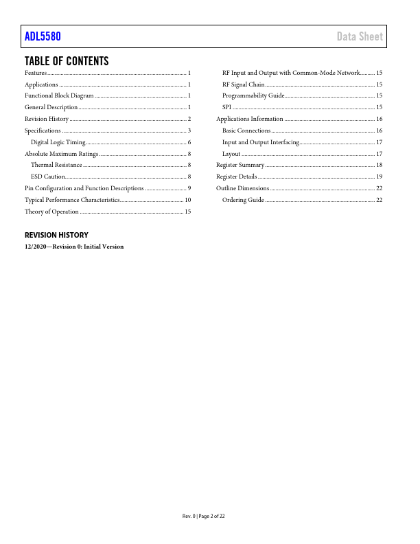
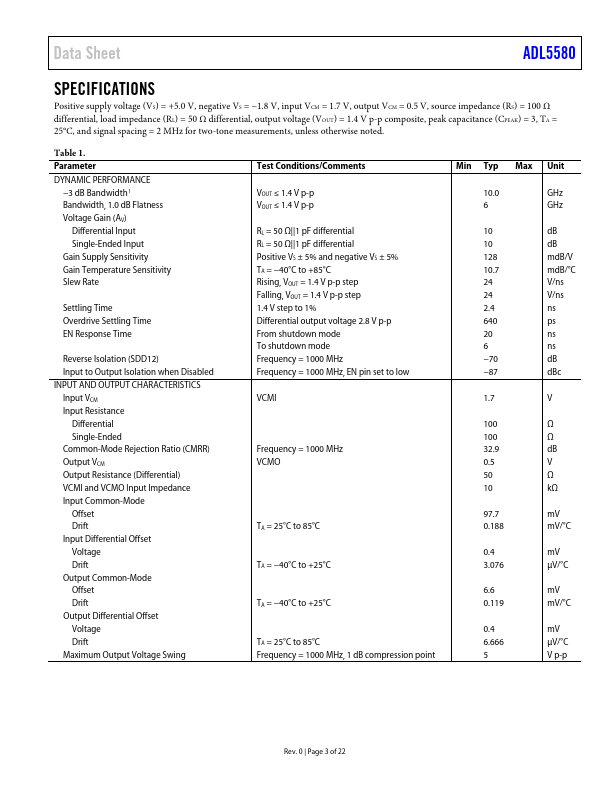
−3 dB bandwidth: 10.0 GHz Preset 10 dB gain, can be reduced by adding external resistors Differential or single-ended input to differential output Internally dc-coupled inputs and outputs Input voltage noise (NSD, RTI): 2.25 nV/√Hz at 100 MHz Low noise input stage: 11.3 dB noise figure at 1 GHz Low distortion with +5.0 V and −1.8 V supplies and 1.4 V p-p output differential with a 50 Ω||1 pF load differential 2 GHz: −59.4 dBc (HD2), −54.3 dBc (HD3), −68.2 dBc (IMD3) 6 GHz: −66 dBc (HD2), −88.1 dBc (HD3), −48.3 dBc (IMD3) 276 mA positive supply current at 5.0 V typical −224 mA negative supply current at −1.8 V typical Power disable APPLICATIONS
Instrumentation and defense applications GENERAL DESCRIPTION
In addition, this device has low distortion for single-ended input driver applications. By using two external series resistors, the gain selection from 10 dB for a differential input can be modified to a lower gain. The device maintains low distortion through its output common-mode voltage (VCM) of 0.5 V, providing a flexible capability for driving ADCs with full-scale levels up to 1.4 V p-p. Analog Devices