Datasheet4U Logo Datasheet4U.com

ADM6820 - (ADM6819 / ADM6820) FET Drive Simple Sequencers

This page provides the datasheet information for the ADM6820, a member of the ADM6819 (ADM6819 / ADM6820) FET Drive Simple Sequencers family.

Description

The ADM6819 and ADM6820 are simple power supply sequencers with FET drive capability for enhancing N-channel MOSFETs.

These devices can monitor a primary supply voltage and enable/disable an external N-channel FET for a secondary supply.

The ADM6819 has the ability to monitor two supplies.

Features

  • Single chip enables power supply sequencing of two supplies On-board charge pump fully enhances N-channel FET Adjustable primary supply monitor to 0.618 V Delay from primary supply to secondary supply enabled Fixed 300 ms delay (ADM6819) Capacitor adjustable delay (ADM6820) Logic/analog driven enable input (ADM6819).
  • 40°C to +85°C operating range Packaged in small 6-lead SOT-23 package Pin-to-pin compatibility with MAX6819/MAX6820 VCC1 VCC2 VCC1 VCC2 CHARGE PUMP UVLO R1 SETV 0.618V LOGIC.

📥 Download Datasheet

Datasheet preview – ADM6820

Datasheet Details

Part number ADM6820
Manufacturer Analog Devices
File Size 186.92 KB
Description (ADM6819 / ADM6820) FET Drive Simple Sequencers
Datasheet download datasheet ADM6820 Datasheet
Additional preview pages of the ADM6820 datasheet.
Other Datasheets by Analog Devices

Full PDF Text Transcription

Click to expand full text
www.DataSheet4U.com FET Drive Simple Sequencers® ADM6819/ADM6820 FEATURES Single chip enables power supply sequencing of two supplies On-board charge pump fully enhances N-channel FET Adjustable primary supply monitor to 0.618 V Delay from primary supply to secondary supply enabled Fixed 300 ms delay (ADM6819) Capacitor adjustable delay (ADM6820) Logic/analog driven enable input (ADM6819) −40°C to +85°C operating range Packaged in small 6-lead SOT-23 package Pin-to-pin compatibility with MAX6819/MAX6820 
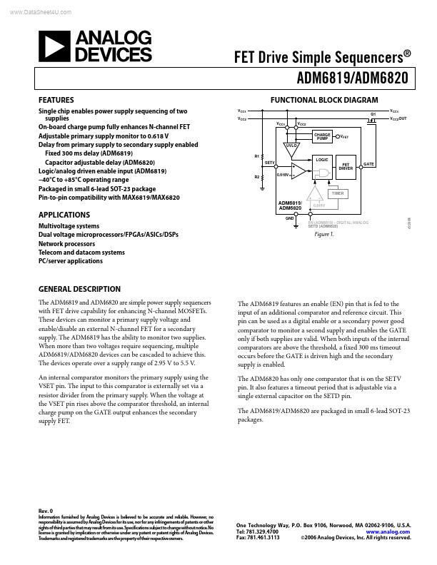
VCC1 VCC2 VCC1 VCC2 CHARGE PUMP UVLO R1 SETV 0.618V LOGIC FET DRIVER GATE VFET FUNCTIONAL BLOCK DIAGRAM Q1 VCC1 VCC2 OUT R2 TIMER ADM6819/ ADM6820 0.
Published: |