FEATURES
GENERAL DESCRIPTION
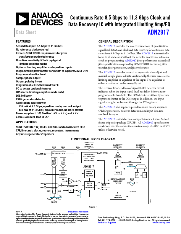
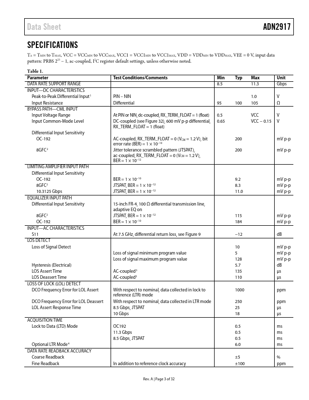
Serial data input: 8.5 Gbps to 11.3 Gbps No reference clock required Exceeds SONET/SDH requirements for jitter transfer/generation/tolerance Quantizer sensitivity: 9.2 mV p-p typical (limiting amplifier mode) Optional limiting amplifier and equalizer inputs Programmable jitter transfer bandwidth to support G.8251 OTN Programmable slice level Sample phase adjust Output polarity invert Programmable LOS threshold via I2C I2C to access optional features LOS alarm (limiting amplifier mode only) LOL indicator PRBS generator/detector Application-aware power 352 mW at 8.5 Gbps, equalizer mode, no clock output 430 mW at 11.3 Gbps, equalizer mode, no clock output Power supplies: 1.2 V, flexible 1.8 V to 3.3 V, and 3.3 V 4 mm × 4 mm 24-lead LFCSP APPLICATIONS
SONET/SDH OC-192, 10GFC, and 10GE and all associated FECs XFP, line cards, clocks, routers, repeaters, instruments Any rate regenerators/repeaters ADN2917 jitter performance exceeds all jitter specifications required by SONET/SDH, including jitter transfer, jitter generation, and jitter tolerance. Analog Devices