Datasheet4U Logo Datasheet4U.com

ADN4670 - Programmable Low Voltage 1:10 LVDS Clock Driver

Description

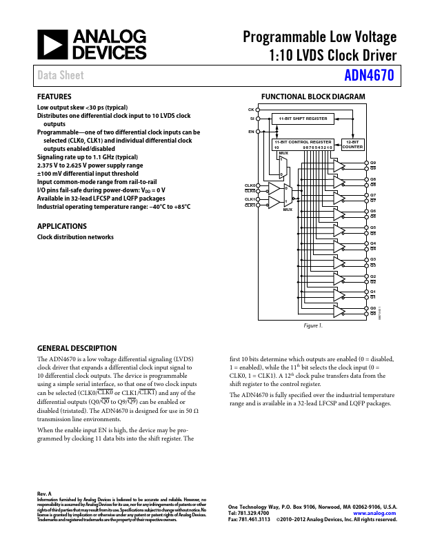
The ADN4670 is a low voltage differential signaling (LVDS) clock driver that expands a differential clock input signal to 10 differential clock outputs.

Features

  • Low output skew.

📥 Download Datasheet

Datasheet Details

Part number ADN4670
Manufacturer Analog Devices
File Size 269.49 KB
Description Programmable Low Voltage 1:10 LVDS Clock Driver
Datasheet download datasheet ADN4670 Datasheet

Full PDF Text Transcription (Reference)

The following content is an automatically extracted verbatim text from the original manufacturer datasheet and is provided for reference purposes only.

View original datasheet text
Data Sheet FEATURES Low output skew <30 ps (typical) Distributes one differential clock input to 10 LVDS clock outputs Programmable—one of two differential clock inputs can be selected (CLK0, CLK1) and individual differential clock outputs enabled/disabled Signaling rate up to 1.1 GHz (typical) 2.375 V to 2.625 V power supply range ±100 mV differential input threshold Input common-mode range from rail-to-rail I/O pins fail-safe during power-down: VDD = 0 V Available in 32-lead LFCSP and LQFP packages Industrial operating temperature range: −40°C to +85°C APPLICATIONS Clock distribution networks GENERAL DESCRIPTION The ADN4670 is a low voltage differential signaling (LVDS) clock driver that expands a differential clock input signal to 10 differential clock outputs.
Published: |