The following content is an automatically extracted verbatim text
from the original manufacturer datasheet and is provided for reference purposes only.
View original datasheet text
Data Sheet
FEATURES
Low RDSON of 40 mΩ Wide input voltage range: 2.3 V to 13.2 V 2 A continuous operating current, TJ = <85°C 1.2 V logic compatible enable input Low 15 µA quiescent current, VIN = 3.3 V Low 19 µA quiescent current, VIN = 6.5 V Ultralow shutdown current: 2.0 µA at VIN = 6.5 V Ultrasmall 1.0 mm × 1.5 mm, 6-ball, 0.5 mm pitch WLCSP
APPLICATIONS
Mobile phones Digital cameras and audio devices Portable and battery-powered equipment
GENERAL DESCRIPTION
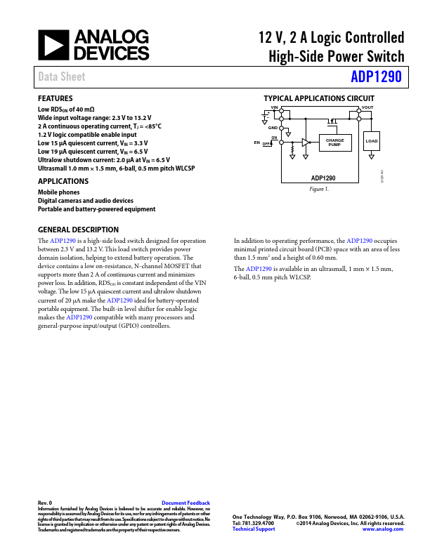
The ADP1290 is a high-side load switch designed for operation between 2.3 V and 13.2 V. This load switch provides power domain isolation, helping to extend battery operation. The device contains a low on-resistance, N-channel MOSFET that supports more than 2 A of continuous current and minimizes power loss.