ADP2140
ADP2140 is Low Quiescent Current Buck manufactured by Analog Devices.
FEATURES
Input voltage range: 2.3 V to 5.5 V LDO input (VIN2) 1.65 V to 5.5 V Buck output voltage range: 1.0 V to 3.3 V LDO output voltage range: 0.8 V to 3.3 V Buck output current: 600 m A LDO output current: 300 m A LDO quiescent current: 22 μA with zero load Buck quiescent current: 20 μA in PSM mode Low shutdown current: <0.3 μA Low LDO dropout 110 m V @ 300 m A load High LDO PSRR
65 d B @ 10 k Hz at VOUT2 = 1.2 V 55 d B @ 100 k Hz at VOUT2 = 1.2 V Low noise LDO: 40 μV rms at VOUT2 = 1.2 V Initial accuracy: ±1% Current-limit and thermal overload protection Power-good indicator Optional enable sequencing 10-lead 0.75 mm × 3 mm × 3 mm LFCSP package
APPLICATIONS
Mobile phones Personal media players Digital camera and audio devices Portable and battery-powered equipment
GENERAL DESCRIPTION
The ADP2140 includes a high efficiency, low quiescent 600 m A stepdown dc-to-dc converter and a 300 m A LDO packaged in a small 10-lead 3 mm × 3 mm LFCSP. The total solution requires only four tiny external ponents.
The buck regulator uses a proprietary high speed currentmode, constant frequency, pulse-width modulation (PWM) control scheme for excellent stability and transient response. To ensure the longest battery life in portable applications, the ADP2140 has a power saving variable frequency mode to reduce switching frequency under light loads.
The LDO is a low quiescent current, low dropout linear regulator designed to operate in a split supply mode with VIN2 as low as 1.65 V. The low input voltage minimum allows the LDO to be powered from the output of the buck regulator increasing efficiency and reducing power dissipation. The ADP2140 runs from input voltages of 2.3 V to 5.5 V allowing single Li+/Li- polymer cell, multiple alkaline/Ni MH cell, PCMCIA, and other standard power sources.
07932-001
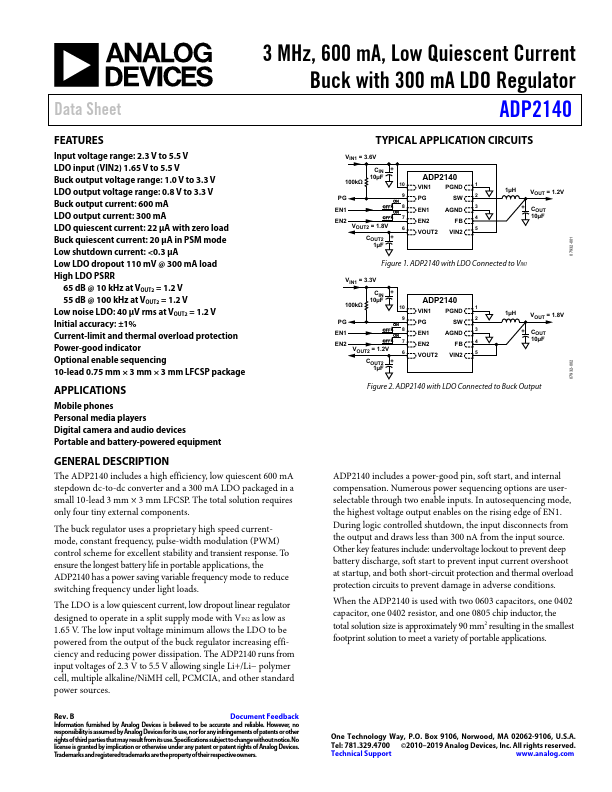
TYPICAL APPLICATION CIRCUITS
VIN1 = 3.6V
100kΩ
CIN 10µF
+
VIN1 PGND
SW 2
EN1
EN1
AGND 3
EN2
EN2
FB 4
VOUT2 = 1.8V
VOUT2 VIN2 5
COUT2...