ADP3089
ADP3089 is 1A Buck Regulator manufactured by Analog Devices.
FEATURES
1 MHz PWM Frequency Ultrasmall 8-lead 3×3 Sq. mm Chip Scale Package Automatic PWM to Power Saving Mode at Light Load Fully Integrated 1.5 A Power Switch 3% Output Regulation Accuracy over Temperature, Line, and Load 100% Duty Cycle Operation .. Simple pensation Output Voltage: 1.25 V to 11.5 V Input Voltage: up to 12 V Small Inductor and MLC Capacitors Low Quiescent Current while Pulse Skipping Thermal Shutdown Fully Integrated Soft Start Cycle-by-cycle Current Limit APPLICATONS PDAs and Palmtop puters Notebook puters PCMCIA Cards Bus Products Portable Instruments Industrial Systems GENERAL DESCRIPTION
IN IN
1 MHz, 1 A Buck Regulator ADP3089
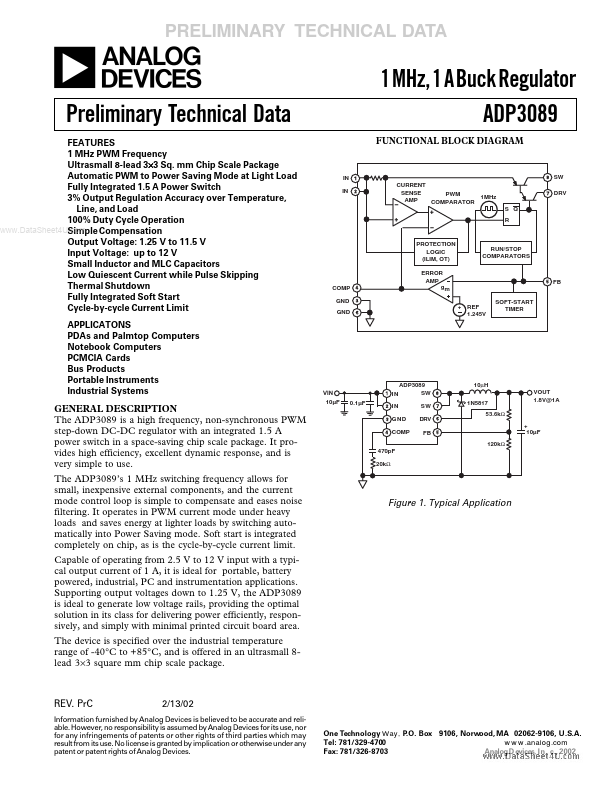
FUNCTIONAL BLOCK DIAGRAM
SW CURRENT SENSE PWM 1MHz AMP PARATOR S Q R DRV
PROTECTION LOGIC (ILIM, OT) ERROR AMP gm
RUN/STOP PARATORS
FB SOFT-START TIMER
P GND GND
+ REF 1.245V
VIN 10µF 0.1µF
IN IN
ADP3089 SW SW DRV FB
10µH 1N5817 53.6kΩ + 10µF 120kΩ VOUT 1.8V@1A
The ADP3089 is a high frequency, non-synchronous PWM step-down DC-DC regulator with an integrated 1.5 A power switch in a space-saving chip scale package. It provides high efficiency, excellent dynamic response, and is very simple to use. The ADP3089’s 1 MHz switching frequency allows for small, inexpensive external ponents, and the current mode control loop is simple to pensate and eases noise filtering. It operates in PWM current mode under heavy loads and saves energy at lighter loads by switching automatically into Power Saving mode. Soft start is integrated pletely on chip, as is the cycle-by-cycle current limit. Capable of operating from 2.5 V to 12 V input with a typical output current of 1 A, it is ideal for portable, battery powered, industrial, PC and instrumentation applications. Supporting output voltages down to 1.25 V, the ADP3089 is ideal to generate low voltage rails, providing the optimal solution in its class for delivering power efficiently, responsively, and simply with minimal printed circuit board area. The device is specified...