FEATURES
Wide input voltage range: 2.85 V to 15 V Adjustable negative output to VIN − 39 V Integrated 800 mA main switch 1.2 MHz/2.4 MHz switching frequency with optional external frequency synchronization from 1.0 MHz to 2.6 MHz Resistor programmable soft start timer Slew rate control for lower system noise Precision enable control UVLO, OCP, OVP, and TSD protection 1.61 mm × 2.18 mm, 12-ball WLCSP −40°C to +125°C junction temperature range Supported by the ADIsimPower tool set APPLICATIONS
Bipolar amplifiers, analog-to-digital converters (ADCs), digital-to-analog converters (DACs), and multiplexers Charge coupled device (CCD) bias supplies Optical module supplies Radio frequency (RF) power amplifier (PA) bias GENERAL DESCRIPTION
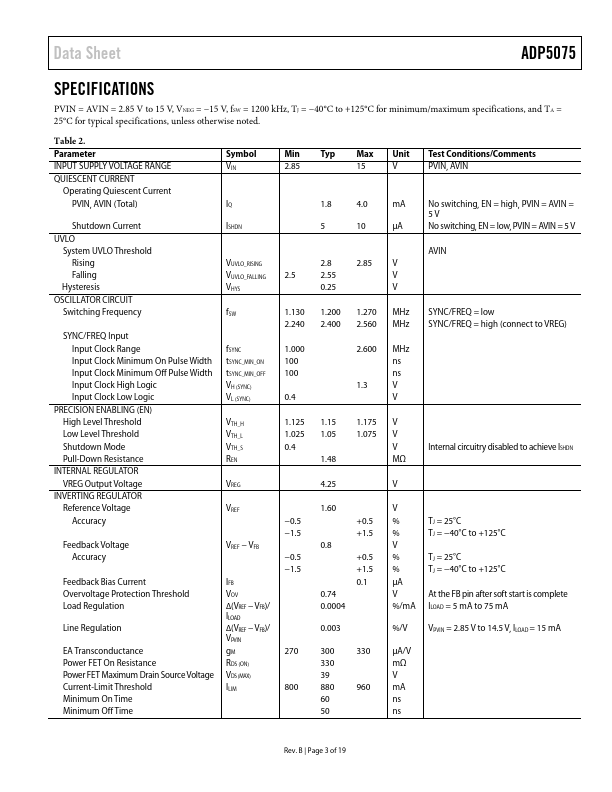
The ADP5075 operates at a pin selected 1.2 MHz/2.4 MHz switching frequency. The ADP5075 can synchronize with an external oscillator from 1.0 MHz to 2.6 MHz to ease noise filtering in sensitive applications. The regulator implements programmable slew rate control circuitry for the MOSFET driver stage to reduce electromagnetic interference (EMI). Analog Devices