ADUC702
ADUC702 is Precision Analog Microcontroller 12-bit Analog I/O/ ARM7TDMI MCU manufactured by Analog Devices.
- Part of the ADU comparator family.
- Part of the ADU comparator family.
FEATURES
Analog I/O Multi-Channel, 12-bit, 1MSPS ADC
- Up to 16 ADC channels
- Fully differential and single-ended modes 0 to VREF Analog Input Range 12-bit Voltage Output DACs
- Up to 4 DAC outputs available- On-Chip 20ppm/°C Voltage Reference On-Chip Temperature Sensor (±3°C) Unmitted Voltage parator
Microcontroller ARM7TDMI Core, 16/32-bit RISC architecture JTAG Port supports code download and debug
Clocking options:
- Trimmed On-Chip Oscillator (± 3%)
- External Watch crystal
- External clock source
45MHz PLL with Programmable Divider Memory
62k Bytes Flash/EE Memory, 8k Bytes SRAM In-Circuit Download, JTAG based Debug Software triggered in-circuit re-programmability On-Chip Peripherals UART, 2 X I2C and SPI Serial I/O Up to 40-Pin GPIO Port-
4 X General Purpose Timers Wake-up and Watchdog Timers Power Supply Monitor Three-phase 16-bit PWM generator- PLA
- Programmable Logic (Array) Power Specified for 3V operation Active Mode: 3m A (@1MHz)
50m A (@45MHz) Packages and Temperature Range
From 40 lead 6x6mm LFCSP to 80 pin LQFP- Fully specified for
- 40°C to 125°C operation Tools Low-Cost Quick Start Development System Full Third-Party Support
- Package, PWM, GPIO availability and number of Analog I/O depend on part model. See page 9.
APPLICATIONS
Industrial Control and Automation Systems Smart Sensors, Precision Instrumentation Base Station Systems, Optical Networking
(See general description on page 11)
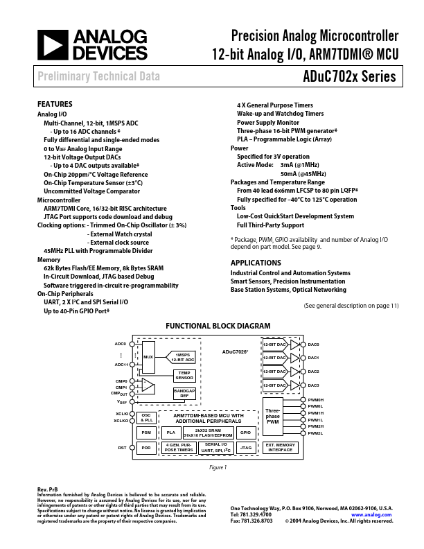
FUNCTIONAL BLOCK DIAGRAM
... ...
ADC0
ADC11
CMP0 CMP1 CMPOUT VREF XCLKI XCLKO
+
- 1MSPS 12-BIT ADC
TEMP SENSOR
BANDGAP REF
ADu C7026-
12-BIT DAC 12-BIT DAC 12-BIT DAC 12-BIT DAC
OSC & PLL
ARM7TDMI-BASED MCU WITH ADDITIONAL PERIPHERALS
2k X32 SRAM 31k X16...