FEATURES
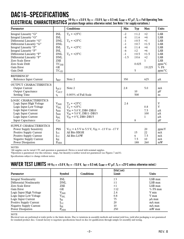
؎1 LSB Differential Linearity (max) Guaranteed Monotonic Over Temperature Range ؎2 LSB Integral Linearity (max) 500 ns Settling Time 5 mA Full-Scale Output TTL/CMOS Compatible Low Power: 190 mW (typ) Available in Die Form APPLICATIONS
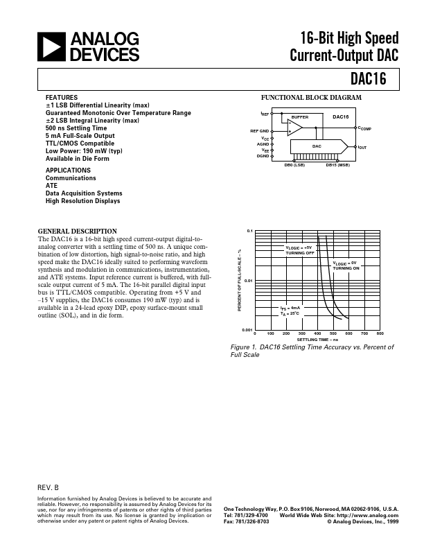
Communications ATE Data Acquisition Systems High Resolution Displays IREF REF GND VCC AGND VEE DGND 16-Bit High Speed Current-Output DAC DAC16 FUNCTIONAL BLOCK DIAGRAM BUFFER DAC16 CCOMP DAC IOUT DB0 (LSB) DB15 (MSB) GENERAL DESCRIPTION
0.1 Input reference current is buffered, with fullscale output current of 5 mA. Operating from +5 V and –15 V supplies, the DAC16 consumes 190 mW (typ) and is available in a 24-lead epoxy DIP, epoxy surface-mount small outline (SOL), and in die form. PERCENT OF FULL-SCALE – % VLOGIC = +5V TURNING OFF VLOGIC = 0V TURNING ON 0.01 IFS = 4mA TA = 25؇C 0.001 0 100 200 300 400 500 SETTLING TIME – ns 600 700 800 Figure 1. DAC16 Settling Time Accuracy vs. Percent of Full Scale REV. B Information furnished by Analog Devices is believed to be accurate and reliable. Analog Devices