FEATURES
Fast, Flexible, Microprocessor Interfacing in Serially Controlled Systems Buffered Digital Output Pin for Daisy-Chaining Multiple DACs Minimizes Address-Decoding in Multiple DAC Systems—Three-Wire Interface for Any Number of DACs One Data Line One CLK Line One Load Line Improved Resistance to ESD –40؇ C to +85؇ C for the Extended Industrial Temperature Range APPLICATIONS
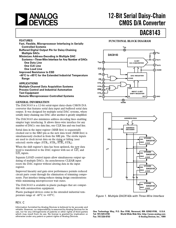
Multiple-Channel Data Acquisition Systems Process Control and Industrial Automation Test Equipment Remote Microprocessor-Controlled Systems GENERAL INFORMATION 12-Bit Serial Daisy-Chain CMOS D/A Converter DAC8143 FUNCTIONAL BLOCK DIAGRAM VDD RFB DAC8143 VREF 12-BIT D/A CONVERTER IOUT1 IOUT2 CLR LD1 LD2 STB1 STB4 STB3 STB2 SRI IN CLK INPUT 12-BIT SHIFT REGISTER OUT SRO AGND DAC REGISTER LOAD DGND It allows three-wire interface for any number of DACs: one data line, one CLK line and one load line. Serial data in the input register (MSB first) is sequentially clocked out to the SRO pin as the new data word (MSB first) is simultaneously clocked in from the SRI pin. Analog Devices