HMC517LC4
Features
Noise Figure: 2.5 d B Gain: 19 d B OIP3: +23 d Bm Single Supply: +3V @ 67 m A 50 Ohm Matched Input/Output Ro HS pliant 4 x 4 mm Package
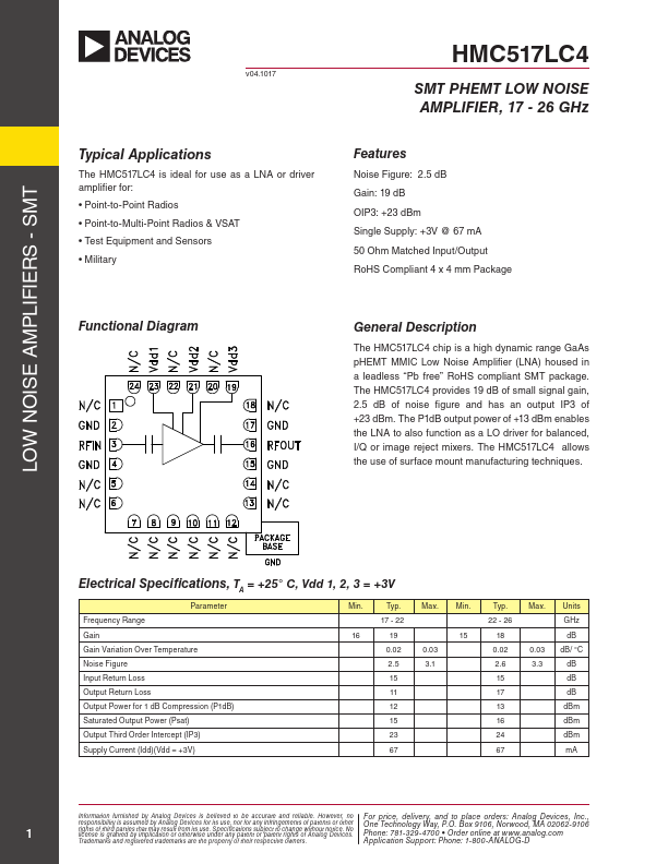
Functional Diagram
General Description
The HMC517LC4 chip is a high dynamic range Ga As p HEMT MMIC Low Noise Amplifier (LNA) housed in a leadless “Pb free” Ro HS pliant SMT package. The HMC517LC4 provides 19 d B of small signal gain, 2.5 d B of noise figure and has an output IP3 of +23 d Bm. The P1d B output power of +13 d Bm enables the LNA to also function as a LO driver for balanced, I/Q or image reject mixers. The HMC517LC4 allows the use of surface mount manufacturing techniques.
Electrical Specifications, TA = +25° C, Vdd 1, 2, 3 = +3V
Parameter Frequency Range Gain Gain Variation Over Temperature Noise Figure Input Return Loss Output Return Loss Output Power for 1 d B pression (P1d B) Saturated Output Power (Psat) Output Third Order Intercept (IP3) Supply Current (Idd)(Vdd = +3V)
Min.
Typ.
Max. Min.
Typ.
Max. Units
- 22
-...