Datasheet4U Logo Datasheet4U.com

HMC987LP5E - LOW NOISE 1:9 FANOUT BUFFER

General Description

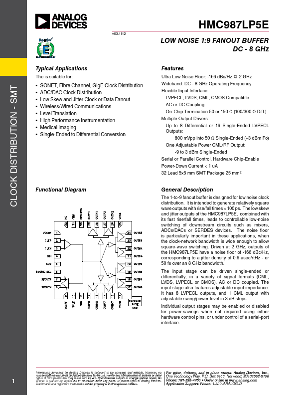
The 1-to-9 fanout buffer is designed for low noise clock distribution.

It is intended to generate relatively square wave outputs with rise/fall times < 100 ps.

Key Features

  • Ultra Low Noise Floor: -166 dBc/Hz @ 2 GHz Wideband: DC - 8 GHz Operating Frequency Flexible Input Interface: LVPECL, LVDS, CML, CMOS Compatible AC or DC Coupling On-Chip Termination 50 or 150 Ω (100/300 Ω Diff. ) Multiple Output Drivers: Up to 8 Differential or 16 Single-Ended LVPECL Outputs: 800 mVpp into 50 Ω Single-Ended (+3 dBm Fo) One Adjustable Power CML/RF Output: -9 to 3 dBm Single-Ended Serial or Parallel Control, Hardware Chip-Enable Power-Down Current < 1 uA 32 Lead 5x5 mm SMT Package.

📥 Download Datasheet

Full PDF Text Transcription (Reference)

The following content is an automatically extracted verbatim text from the original manufacturer datasheet and is provided for reference purposes only.

View original datasheet text
Clock Distribution - SMT v03.1112 Typical Applications The is suitable for: • SONET, Fibre Channel, GigE Clock Distribution • ADC/DAC Clock Distribution • Low Skew and Jitter Clock or Data Fanout • Wireless/Wired Communications • Level Translation • High Performance Instrumentation • Medical Imaging • Single-Ended to Differential Conversion Functional Diagram HMC987LP5E LOW NOISE 1:9 FANOUT BUFFER DC - 8 GHz Features Ultra Low Noise Floor: -166 dBc/Hz @ 2 GHz Wideband: DC - 8 GHz Operating Frequency Flexible Input Interface: LVPECL, LVDS, CML, CMOS Compatible AC or DC Coupling On-Chip Termination 50 or 150 Ω (100/300 Ω Diff.