Analog Devices PM108
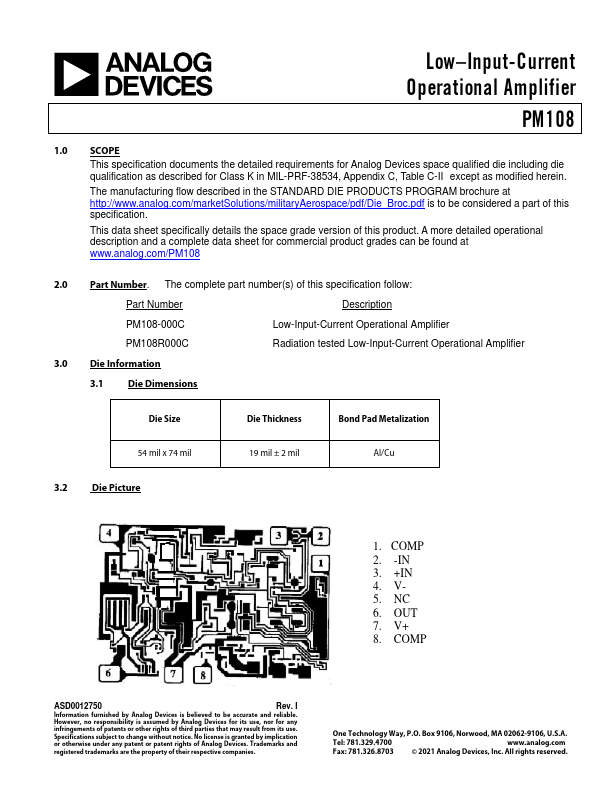
The complete part number(s) of this specification follow: Part Number Description PM108-000C Low-Input-Current Operational Amplifier PM108R000C Radiation tested Low-Input-Current Operational Amplifier 3.0 Die Information 3.1 Die Dimensions Die Size Die Thickness Bond Pad Metalization 54 mil x 74 mil 19 mil ± 2 mil Al/Cu 3.2 Die Picture 1.| Part No. | PM108 |
|---|---|
| Datasheet | PM108 Download |
| Manufacturer |  Analog Devices |
| Description | Low Input Current Operational Amplifier |
| Buy | Stock & Price |
ABSOLUTE MAXIMUM RATINGS
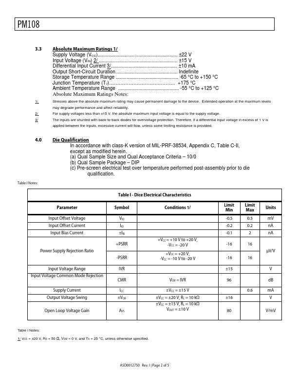
1/ Supply Voltage (VCC)........................................................... ±22 V Input Voltage (VIN) 2/ .......................................................... ±15 V Differential Input Current 3/................................................. ±10 mA Output Short-Circuit Duration.............................................. Indefinite Storage Temperature Range .............................................. -65 °C to +150 °C Junction Temperature (TJ)………………………….………. +175 °C Ambient Temperature Range ............................................. -55 °C to +125 °CABSOLUTE MAXIMUM RATINGS
Notes: 1/ Stresses above the absolute maximum rating may cause permanent damage to the device. Extended operation at the maximum levels may degrade performance and affect reliability. 2/ For supply voltages less than ±15 V, the absolute maximum input voltage is equal to the supply voltage. 3/ The inputs are shunted with back-to-back diodes for overvoltage protection.