ABSOLUTE MAXIMUM RATINGS
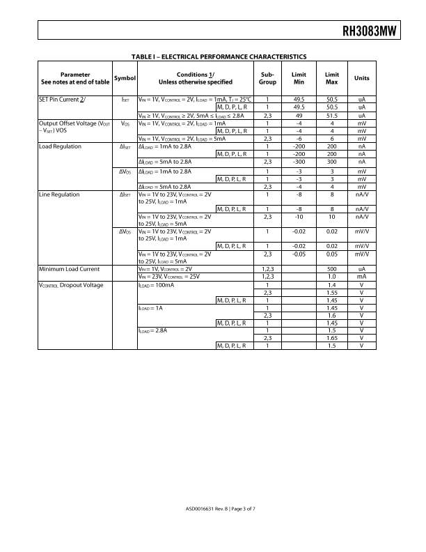
may cause permanent damage to the device. Exposure to absolute maximum ratings for extended periods may affect device reliability. 2/ Output noise is lowered by adding a small capacitor across the voltage setting resistor. Adding this capacitor bypasses the voltage setting resistor shot noise and reference current noise; output noise is then equal to error amplifier noise (see the APPLICATIONS
Information section of commercial datasheet). Table I Notes: 1/ Device supplied to this drawing have been characterized through all levels M, D, P, L, R of irradiation. However, device is only tested at the “R” level. Pre and Post irradiation values are identical unless otherwise specified in Table I. When performing post irradiation electrical measurements for any RHA level, TA = +25°C. 2/ The SET pin is clamped to the output with diodes through 1k resistors. These resistors and diodes will only carry current under transient overloads. Table IIA Notes: 1/ PDA applies to Table I subgroup 1 and 4 and Table IIB delta parameters. Analog Devices