GENERAL DESCRIPTION
The AMP771is designed for precision, low noise, low voltage, and miniature systems. It provides rail-to-rail output swing into heavy loads. The maximum input offset voltage for the AMP771 is TBD µV at room temperature and the input common mode voltage range includes ground. Key Specification Voltage Range VOS(max) VCM(max) Bandwidth Temperature Range 2.7V < VCC < 5.5V TBDµV 0 to VCC – 0.9V 3.5MHz −40° C to 85° C FEATURES
Low Voltage noise Rail-to-rail output APPLICATIONS
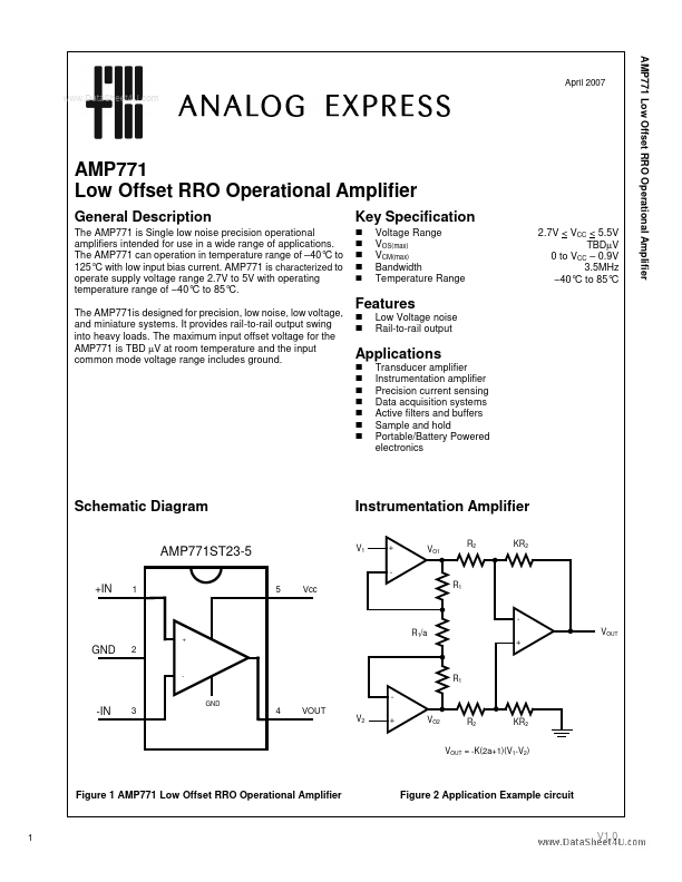
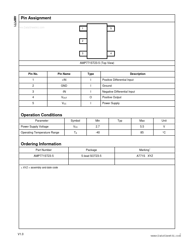
Transducer amplifier Instrumentation amplifier Precision current sensing Data acquisition systems Active filters and buffers Sample and hold Portable/Battery Powered electronics Schematic Diagram AMP771ST23-5 +IN 1 5 Vcc Instrumentation Amplifier V1 + R1 VO1 R2 KR2 + R1/a + VOUT GND 2 - R1 GND - -IN 3 4 VOUT V2 + VO2 R2 KR2 VOUT = -K(2a+1)(V1-V2) Figure 1 AMP771 Low Offset RRO Operational Amplifier Figure 2 Application Example circuit 1 V1.0 AMP771 Pin Assignment 1 5 2 3 4 AMP771ST23-5 (Top View) Pin No. Analog Express