GENERAL DESCRIPTION
The digital logic inputs are 1.8V logic interface compatible with a +2.7V to +3.3V supply. Key Specifications Single Supply Operation High Isolation Low Standby Current Low Crosstalk 3dB Bandwidth at VCC = 5V 1.8V to 5.5V -66dB at 100kHz <50nA <-66dB at 100kHz 10MHz(typ) FEATURES
Ultra Low NC RON, 0.5Ω Max at 2.7V Ultra Low NO RON, 0.8Ω Max at 2.7V Low Distortion, <0.14% THD Full 0-Vcc Signal Handling High Continuous Current Capability APPLICATIONS
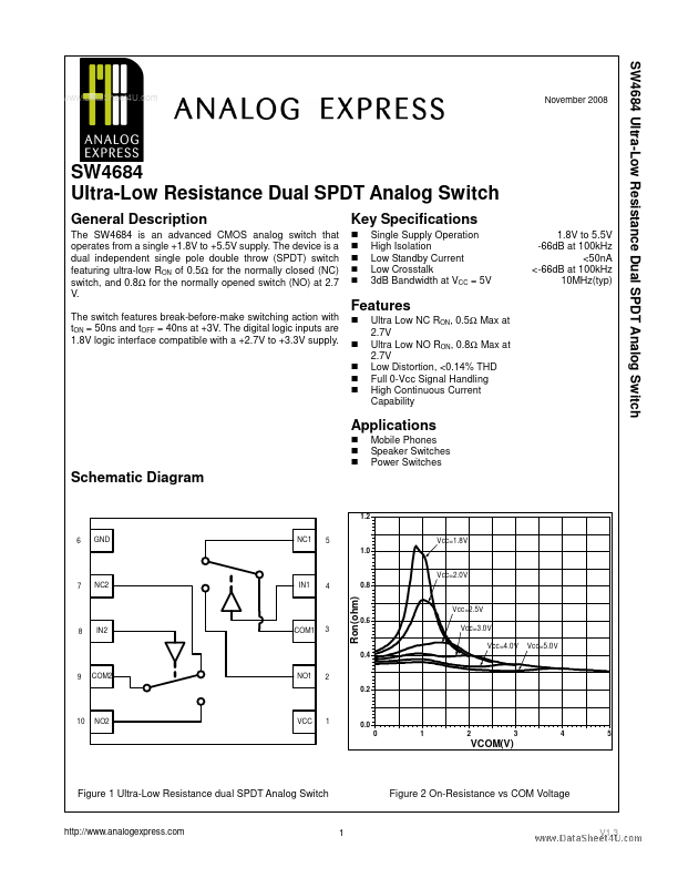
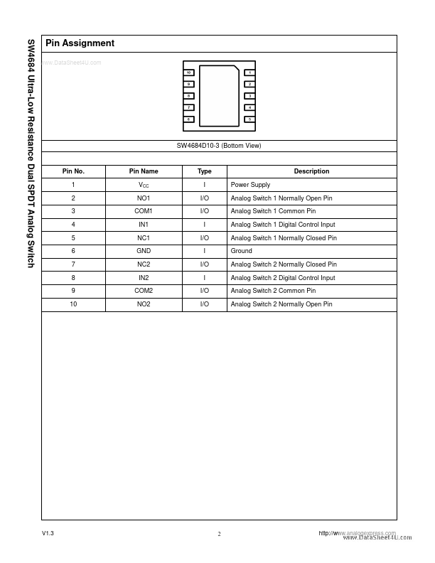
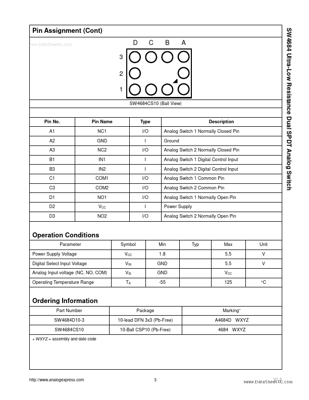
Mobile Phones Speaker Switches Power Switches Schematic Diagram 1.2 6 GND NC1 5 1.0 Vcc=1.8V Vcc=2.0V 7 NC2 IN1 4 0.8 Ron(ohm) Vcc=2.5V 0.6 Vcc=3.0V Vcc=4.0V 0.4 Vcc=5.0V 8 IN2 COM1 3 9 COM2 NO1 2 0.2 10 NO2 VCC 1 0.0 0 1 2 3 4 5 VCOM(V) Figure 1 Ultra-Low Resistance dual SPDT Analog Switch Figure 2 On-Resistance vs COM Voltage 1 V1.3 SW4684 Ultra-Low Resistance Dual SPDT Analog Switch Pin Assignment SW4684D10-3 (Bottom View) Pin No. 1 2 3 4 5 6 7 8 9 10 Pin Name VCC NO1 COM1 IN1 NC1 GND NC2 IN2 COM2 NO2 Type I I/O I/O I... Analog Express