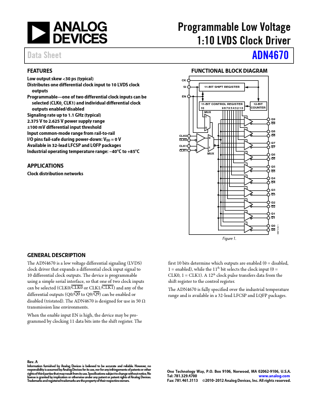
ADN4670 Description
The ADN4670 is a low voltage differential signaling (LVDS) clock driver that expands a differential clock input signal to 10 differential clock outputs. The device is programmable using a simple serial interface, so that one of two clock inputs can be selected (CLK0/CLK0 or CLK1/CLK1) and any of the differential outputs (Q0/Q0 to Q9/Q9) can be enabled or disabled (tris.