APM9935K
APM9935K is Dual P-Channel MOSFET manufactured by Anpec Electronics Coropration.
Features
- -20V/-6A , RDS(ON)=30mΩ(typ.) @ VGS=-4.5V RDS(ON)=38mΩ(typ.) @ VGS=-2.5V
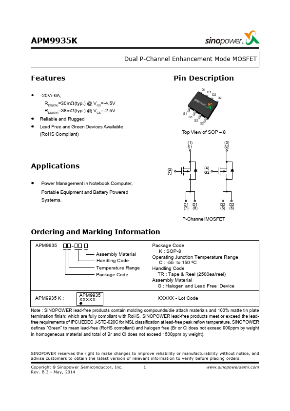
Pin Description
D1 D1 D2 D2
- Super High Dense Cell Design ..
- Reliable and Rugged
- Lead Free Available (Ro HS pliant)
S1 G1 S2 G2
Top View of SOP
- 8
(1) S1 (3) S2
Applications
- Power Management in Notebook puter, Portable Equipment and Battery Powered Systems
(2) G1
(4) G2
D1 (7)
D1 (8)
D2 (5)
D2 (6)
P-Channel MOSFET
Ordering and Marking Information
APM9935 Lead Free Code Handling Code Temp. Range Package Code Package Code K : SOP-8 Operating Junction Temp. Range C : -55 to 150°C Handling Code TU : Tube TR : Tape & Reel Lead Free Code L : Lead Free Device Blank : Original Device XXXXX
- Date Code
APM9935 K :
APM9935 XXXXX
Note: ANPEC lead-free products contain molding pounds/die attach materials and 100% matte in plate termination finish; which are fully pliant with Ro HS and patible with both Sn Pb and lead-free soldiering operations. ANPEC lead-free products meet or exceed the lead-free requirements of IPC/JEDEC J STD-020C for MSL classification at lead-free peak reflow temperature.
ANPEC reserves the right to make changes to improve reliability or manufacturability without notice, and advise customers to obtain the latest version of relevant information to verify before placing orders. Copyright ANPEC Electronics Corp. Rev. B.1
- Mar., 2005 1 .anpec..tw
Absolute Maximum Ratings
Symbol VDSS VGSS ID- IDM- IS-
..
(TA = 25°C unless otherwise noted)
Rating -20 ±12 -6 VGS=-4.5V -20 -2 150 -55 to 150 TA=25°C TA=100°C 2 0.8 62.5 W °C/W V A A °C Unit
Parameter Drain-Source Voltage Gate-Source Voltage Continuous Drain Current 300µs Pulsed Drain Current Diode Continuous Forward Current Maximum Junction Temperature Storage Temperature Range Maximum Power Dissipation Thermal Resistance-Junction to Ambient
TJ TSTG PD- RθJA-
Note:
- Surface Mounted on 1in pad area, t ≤ 10sec.
Electrical Characteristics
Symbol...