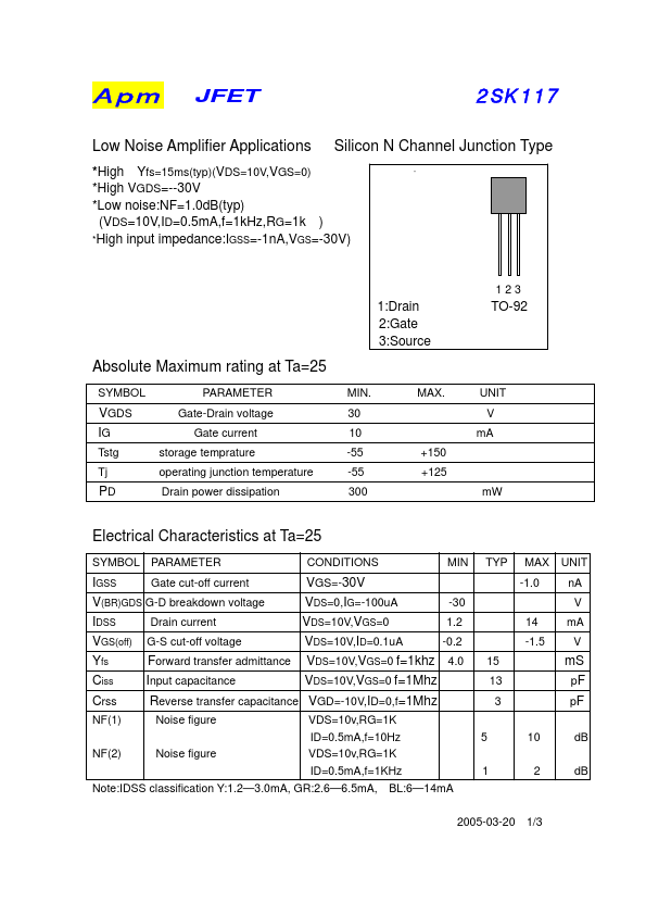
Click to expand full text
Apm JFET
2SK117
Low Noise Amplifier Applications Silicon N Channel Junction Type
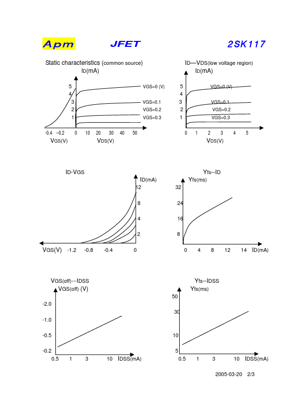
*High Yfs=15ms(typ)(VDS=10V,VGS=0) *High VGDS=--30V *
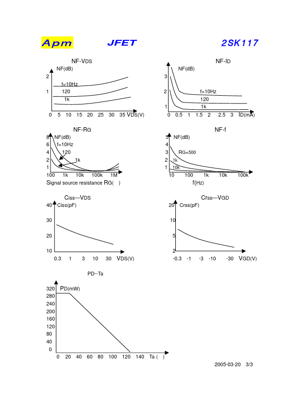
Low noise:NF=1.0dB(typ)
(VDS=10V,ID=0.5mA,f=1kHz,RG=1k ) *High input impedance:IGSS=-1nA,VGS=-30V)
Absolute Maximum rating at Ta=25
SYMBOL
VGDS IG
Tstg Tj
PD
PARAMETER Gate-Drain voltage
Gate current storage temprature operating junction temperature Drain power dissipation
1:Drain 2:Gate 3:Source
MIN. 30 10 -55 -55 300
MAX.
+150 +125
123
TO-92
UNIT V
mA
mW
Electrical Characteristics at Ta=25
SYMBOL PARAMETER
CONDITIONS
MIN
IGSS
Gate cut-off current
VGS=-30V
V(BR)GDS G-D breakdown voltage
VDS=0,IG=-100uA
-30
IDSS
Drain current
VDS=10V,VGS=0
1.2
VGS(off) G-S cut-off voltage
VDS=10V,ID=0.1uA
-0.