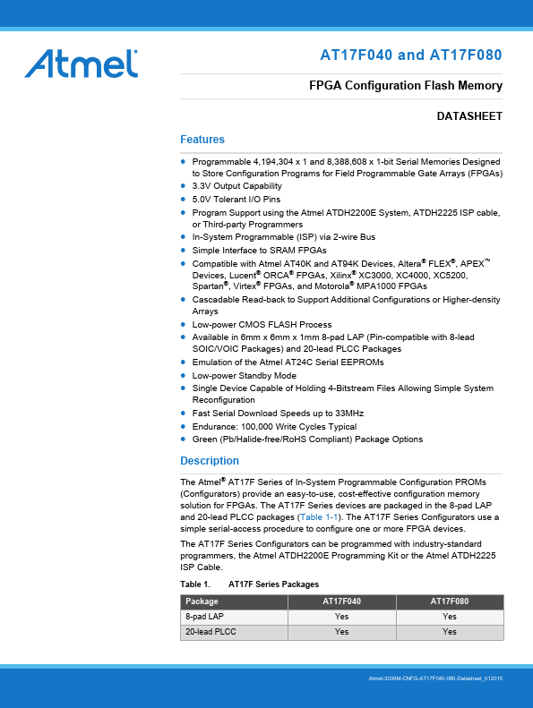
Atmel AT17F040
FPGA Configuration Flash Memory
| Part No. | AT17F040 |
|---|---|
| Datasheet | AT17F040 Download |
| Manufacturer |  Atmel |
| Description | FPGA Configuration Flash Memory |
| Buy | Stock & Price |
FEATURES
● Programmable 4,194,304 x 1 and 8,388,608 x 1-bit Serial Memories Designed to Store Configuration Programs for Field Programmable Gate Arrays (FPGAs)● 3.3V Output Capability
● 5.0V Tolerant I/O Pins
● Program Support using the Atmel ATDH2200E System, ATDH2225 ISP cable, or Third-party Programmers
● In-System Programmable (ISP) via 2-wire Bus
● Simple Interface to SRAM FPGAs
● Compatible with Atmel AT40K and AT94K Devices, Altera® FLEX®, APEX™ Devices, Lucent® ORCA® FPGAs, Xilinx® XC3000, XC4000, XC5200, Spartan®, Virtex® FPGAs, and Motorola® MPA1000 FPGAs
● Cascadable Read-back to Support Additional Configurations or Higher-density Arrays
● Low-power CMOS FLASH Process
● Available in 6mm x 6mm x 1mm 8-pad LAP (Pin-compatible with 8-lead SOIC/VOIC Packages) and 20-lead PLCC Packages
● Emulation of the Atmel AT24C Serial EEPROMs
● Low-power Standby Mode
● Single Device Capabl