AT49F001A Overview
Key Specifications
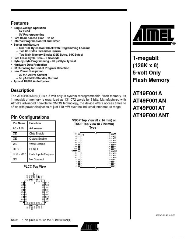
Package: PLCC
Mount Type: Surface Mount
Pins: 32
Operating Voltage: 5 V
Description
The AT49F001A(N)(T) is a 5-volt only in-system reprogrammable Flash memory. Its 1 megabit of memory is organized as 131,072 words by 8 bits.
Key Features
- Single-voltage Operation
- 1-megabit (128K x