AS5C4009LL
AS5C4009LL is 512K x 8 SRAM manufactured by Austin Semiconductor.
FEATURES
- Ultra Low Power with 2V Data Retention (0.2m W MAX worst case Power-down standby)
- Fully Static, No Clocks
- Single +5V ±10% power supply
- Easy memory expansion with CE and OE options
- All inputs and outputs are TTL-patible
- Three state outputs
- Operating temperature range: Ceramic -55o C to +125o C & -40o C to +85o C Plastic -40o C to +85o C3
1. Not applicable to plastic package 2. Applies to CW package only. 3. Contact factory for -55o C to +125o C
..
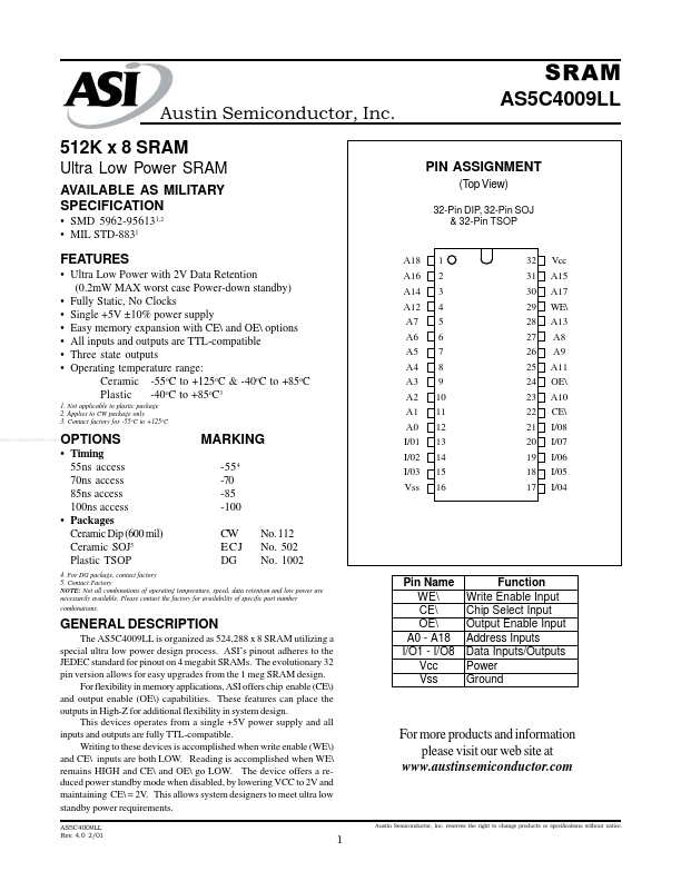
A18 A16 A14 A12 A7 A6 A5 A4 A3 A2 A1 A0
1 2 3 4 5 6 7 8 9 10 11 12 13 14 15 16
32 31 30 29 28 27 26 25 24 23 22 21 20 19 18 17
Vcc A15 A17 WE A13 A8 A9 A11 OE A10 CE I/08 I/07 I/06 I/05 I/04
OPTIONS
- Timing 55ns access 70ns access 85ns access 100ns access
- Packages Ceramic Dip (600 mil) Ceramic SOJ5 Plastic TSOP
MARKING
-55 4 -70 -85 -100 CW ECJ DG No. 112 No. 502 No. 1002
I/01 I/02 I/03 Vss
4. For DG package, contact factory 5. Contact Factory NOTE: Not all binations of operating temperature, speed, data retention and low power are necessarily available. Please contact the factory for availability of specific part number binations.
GENERAL DESCRIPTION
The AS5C4009LL is organized as 524,288 x 8 SRAM utilizing a special ultra low power design process. ASI’s pinout adheres to the JEDEC standard for pinout on 4 megabit SRAMs. The evolutionary 32 pin version allows for easy upgrades from the 1 meg SRAM design. For flexibility in memory applications, ASI offers chip enable (CE) and output enable (OE) capabilities. These features can place the outputs in High-Z for additional flexibility in system design. This devices operates from a single +5V power supply and all inputs and outputs are fully TTL-patible. Writing to these devices is acplished when write enable (WE) and CE inputs are both LOW. Reading is acplished when WE remains HIGH and CE and OE go LOW. The device offers a reduced power standby mode when disabled, by lowering VCC to 2V and maintaining CE = 2V. This allows system designers to meet...