AS5LC512K8
AS5LC512K8 is 512K x 8 SRAM 3.3 VOLT HIGH SPEED SRAM manufactured by Austin Semiconductor.
FEATURES
- Ultra High Speed Asynchronous Operation
- Fully Static, No Clocks
- Multiple center power and ground pins for improved noise immunity
- Easy memory expansion with CE and OE options
- All inputs and outputs are TTL-patible
- Single +3.3V Power Supply +/- 0.3%
- Data Retention Functionality Testing
- Cost Efficient Plastic Packaging
- Extended Testing Over -55ºC to +125ºC for plastics ..
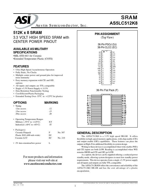
36-Pin Flat Pack (F)
OPTIONS
- Timing 12ns access 15ns access 20ns access
- Operating Temperature Ranges Military (-55o C to +125o C) Industrial (-40o C to +85o C)
- Package(s) Ceramic Flatpack Plastic SOJ (400 mils wide) Ceramic LCC
- 2V data retention/low power
MARKING
-12 -15 -20
XT IT
F DJ EC L
No. 307 No. 210
GENERAL DESCRIPTION
The AS5LC512K8 is a 3.3V high speed SRAM. It offers flexibility in high-speed memory applications, with chip enable (CE) and output enable (OE) capabilities. These features can place the outputs in High-Z for additional flexibility in system design. Writing to these devices is acplished when write enable (WE) and CE inputs are both LOW. Reading is acplished when WE remains HIGH and CE and OE go LOW. As a option, the device can be supplied offering a reduced power standby mode, allowing system designers to meet low standby power requirements. This device operates from a single +3.3V power supply and all inputs and outputs are fully TTL-patible. The AS5LC512K8DJ offers the convenience and reliability of the AS5LC512K8 SRAM and has the cost advantage of a plastic encapsulation.
For more products and information please visit our web site at .austinsemiconductor.
AS5LC512K8 Rev. 1.0 7/02
Austin Semiconductor, Inc. reserves the right to change products or specifications without notice.
SRAM
Austin Semiconductor, Inc.
FUNCTIONAL BLOCK DIAGRAM
VCC GND
DQ8
INPUT BUFFER ROW DECODER I/O CONTROLS
4,194,304-BIT MEMORY ARRAY 1024 ROWS X 4096 COLUMNS
A0-A18
DQ1
COLUMN DECODER
OE WE
- POWER...