Austin Semiconductor AS5SS256K18
The Austin Semiconductor, Inc. The synchronous inputs include all addresses, all data inputs, active LOW chip enable (CE\), two additional chip enables for easy depth expansion (CE2\, AS5SS256K18 Rev.| Part No. | AS5SS256K18 |
|---|---|
| Datasheet | AS5SS256K18 Download |
| Manufacturer |  Austin Semiconductor |
| Description | 256K x 18 SSRAM Synchronous Burst SRAM |
| Buy | Stock & Price |
FEATURES
● Fast access times: 8, 10, and 15ns● Fast clock speed: 113, 100, and 66 MHz
● Fast clock and OE\ access times
● Single +3.3V +0.3V/-0.165V power supply (VDD)
● SNOOZE MODE for reduced-power standby
● Common data inputs and data outputs
● Individual BYTE WRTIE control and GLOBAL WRITE
● Three chip enables for simple depth expansion and address pipelining
● Clock-controlled and registered addresses, data I/Os and control signals
● Interally self-timed WRITE cycle
● Burst control pin (interleaved or linear burst)
● Automatic power-down
● Low capacitive bus loading
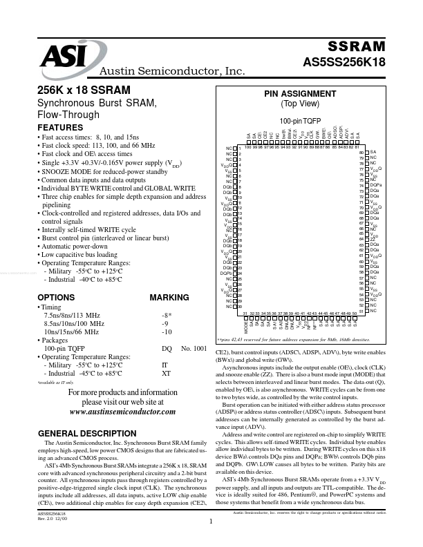
● Operating Temperature Ranges: - Military -55oC to +125oC - Industrial -40oC to +85oC NC NC NC V DD Q VSS NC NC DQb DQb VSS V DD Q DQb DQb VSS V DD NC VSS DQb DQb V DD Q VSS DQb DQb DQPb NC VSS V DD Q NC NC NC AS5SS256K18 PIN ASSIGNMENT (Top View) 100-pin TQFP SA SA CE\ CE2 NC NC bwB\ BWa\ CE2\ V DD VSS CLK GW\ BWE\ OE\ ADSC\ ADSP\ ADV\ SA SA OPTIONS
● Timing 7.5ns/8ns/113 MHz 8.5ns/10ns/100 MHz 10ns/15ns/66 MHz
● Packages 100-pin TQFP
● Operating Temperature Ranges: - Military -55oC to +125oC - Industrial -45oC to +85oC *available as IT only.