MT4C4001J
MT4C4001J is 1 MEG x 4 DRAM Fast Page Mode DRAM manufactured by Austin Semiconductor.
FEATURES
- Industry standard x4 pinout, timing, functions, and packages
- High-performance, CMOS silicon-gate process
- Single +5V±10% power supply
- Low-power, 2.5m W standby; 300m W active, typical
- All inputs, outputs, and clocks are fully TTL and CMOS patible
- 1,024-cycle refresh distributed across 16ms
- Refresh modes: RAS-ONLY, CAS-BEFORE-RAS (CBR), and HIDDEN
- FAST PAGE MODE access cycle
- CBR with WE a HIGH (JEDEC test mode capable via WCBR)
..
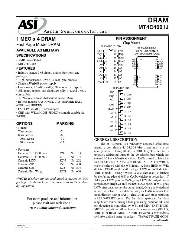
A0 A1 A2 A3 Vcc
9 10 11 12 13
18 17 16 15 14
A8 A7 A6 A5 A4
20-Pin DIP (CZ) OE 1 DQ3 3 Vss 5 2 CAS 4 DQ4 6 DQ1 8 WE 10 A9 12 A1 14 A3 16 A4 18 A6 20 A8
DQ2 7 RAS 9
A0 11 A2 13 Vcc 15 A5 17 A7 19
OPTIONS
- Timing 70ns access 80ns access 100ns access 120ns access
- Packages Ceramic DIP (300 mil) Ceramic DIP (400 mil) Ceramic LCC- Ceramic ZIP Ceramic SOJ Ceramic Gull Wing
MARKING
-7 -8 -10 -12
GENERAL DESCRIPTION
The MT4C4001J is a randomly accessed solid-state memory containing 4,194,304 bits organized in a x4 configuration. During READ or WRITE cycles each bit is uniquely addressed through the 20 address bits which are entered 10 bits (A0-A9) at a time. RAS is used to latch the first 10 bits and CAS the later 10 bits. A READ or WRITE cycle is selected with the WE input. A logic HIGH on WE dictates READ mode while a logic LOW on WE dictates WRITE mode. During a WRITE cycle, data-in (D) is latched by the falling edge of WE or CAS, whichever occurs last. If WE goes LOW prior to CAS going LOW, the output pin(s) remain open (High-Z) until the next CAS cycle. If WE goes LOW after data reaches the output pin(s), Qs are activated and retain the selected cell data as long as CAS remains low (regardless of WE or RAS). This LATE WE pulse results in a READ-WRITE cycle. The four data inputs and four data outputs are routed through four pins using mon I/O and pin direction is controlled by WE and OE. FAST-PAGEMODE operations allow faster data operations (READ, WRITE, or READ-MODIFY-WRITE) within a row address (A0-A9)...