HMMC-5026 Overview
Key Specifications
Package: Module
Max Frequency: 26.5 GHz
Max Operating Temp: 150 °C
Min Operating Temp: -55 °C
Description
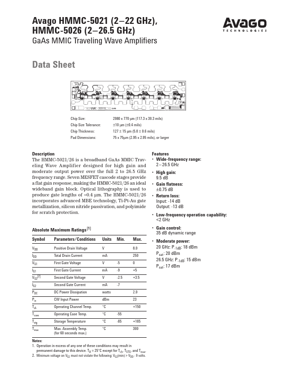
The HMMC-5021/26 is a broadband GaAs MMIC Traveling Wave Amplifier designed for high gain and moderate output power over the full 2 to 26.5 GHz frequency range. Seven MESFET cascode stages provide a flat gain response, making the HMMC-5021/26 an ideal wideband gain block.
Key Features
- Wide-frequency range: 2 – 26.5 GHz
- High gain: 9.5 dB
- Gain flatness: ±0.75 dB
- Return loss: Input: -14 dB Output: -13 dB
- Low-frequency operation capability: <2 GHz
- Gain control: 35 dB dynamic range