Datasheet4U Logo Datasheet4U.com

AX20NV2G6 - NAND Flash Memory

Download the AX20NV2G6 datasheet PDF. This datasheet also covers the AX20NV2G8 variant, as both devices belong to the same nand flash memory family and are provided as variant models within a single manufacturer datasheet.

General Description

3 Ordering Options 4 Valid Combinations Standard 4 Signal Description and Assignment 5 Package Options 6 48-Pin TSOP (Top View) 6 63-Ball FBGA (Balls Down, Top View) 7 Architecture 8 Status Register 11 Bus Interface 17 Standby 17 Busy 17 Device Protection (Write Protect WP#) 17 Co

Key Features

  • Interface.
  • Open NAND Flash Interface (ONFI 1.0) compliant.
  • x8, x16.
  • Technology.
  • Single-level cell (SLC).
  • 3xnm NAND Process.
  • Operating Voltage Range.
  • VCC: 2.70V.
  • 3.60V.
  • Operating Temperature Range.
  • Industrial: -40°C to 85°C.
  • Packages.
  • 48-pin TSOP (12.0mm x 20mm).
  • 63-ball FBGA (9mm x 11mm).
  • Device Signature.
  • Manufacturer’s ID.
  • Device ID.
  • Device Parameters.
  • Unique ID.

📥 Download Datasheet

Note: The manufacturer provides a single datasheet file (AX20NV2G8-Axia.pdf) that lists specifications for multiple related part numbers.

Datasheet Details

Part number AX20NV2G6
Manufacturer Axia
File Size 1.20 MB
Description NAND Flash Memory
Datasheet download datasheet AX20NV2G6 Datasheet

Full PDF Text Transcription (Reference)

The following content is an automatically extracted verbatim text from the original manufacturer datasheet and is provided for reference purposes only.

View original datasheet text
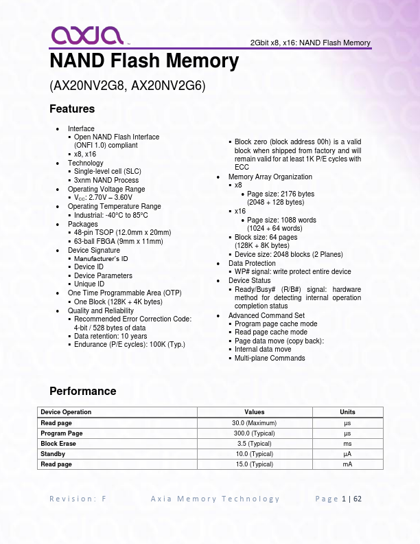
2Gbit x8, x16: NAND Flash Memory NAND Flash Memory (AX20NV2G8, AX20NV2G6) Features • Interface ▪ Open NAND Flash Interface (ONFI 1.0) compliant ▪ x8, x16 • Technology ▪ Single-level cell (SLC) ▪ 3xnm NAND Process • Operating Voltage Range ▪ VCC: 2.70V – 3.60V • Operating Temperature Range ▪ Industrial: -40°C to 85°C • Packages ▪ 48-pin TSOP (12.0mm x 20mm) ▪ 63-ball FBGA (9mm x 11mm) • Device Signature ▪ Manufacturer’s ID ▪ Device ID ▪ Device Parameters ▪ Unique ID • One Time Programmable Area (OTP) ▪ One Block (128K + 4K bytes) • Quality and Reliability ▪ Recommended Error Correction Code: 4-bit / 528 bytes of data ▪ Data retention: 10 years ▪ Endurance (P/E cycles): 100K (Typ.