AZ7500B Overview
Key Specifications
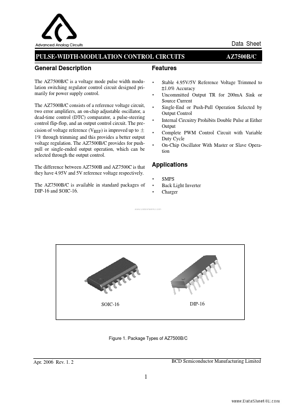
Package: SOIC
Max Operating Temp: 85 °C
Min Operating Temp: -40 °C
Key Features
- Stable 4.95V/5V Reference Voltage Trimmed to ±1.0% Accuracy Uncommitted Output TR for 200mA Sink or Source Current Single-End or Push-Pull Operation Selected by Output Control Internal Circuitry Prohibits Double Pulse at Either Output Complete PWM Control Circuit with Variable Duty Cycle On-Chip Oscillator With Master or Slave Operation
- SMPS Back Light Inverter Charger