BCD Semiconductor Manufacturing Limited AZ7500BP
The AZ7500B/C is a voltage mode pulse width modu- · Stable 4.95V/5V Reference Voltage Trimmed to lation switching regulator control circuit designed pri- ±1.0% Accuracy marily for power supply control. The precision of voltage reference (VREF) is improved up to ± · Output Complete PWM Control Circuit with Variable 1% through trimming and this provides a better output Duty Cycle voltage regulation. The AZ7500B/C provides for push- · On-Chip Oscillator With Master or Slave Opera- pull or single-ended output operation, which can be tion selected through the output control.- Min Voltage : 7V
- Max Voltage : 36V
- Max Operating Temp : 85°C
- Min Operating Temp : -40°C
Source:
Octopart
| Part No. | AZ7500BP |
|---|---|
| Datasheet | AZ7500BP Download |
| Manufacturer |  BCD Semiconductor Manufacturing Limited |
| Description | Pulse-Width-Modulation Controller |
| Buy | Stock & Price |
GENERAL DESCRIPTION
FEATURES
AZ7500B/C● Uncommitted Output TR for 200mA Sink or Source Current The AZ7500B/C consists of a reference voltage circuit,
● Single-End or Push-Pull Operation Selected by two error amplifiers, an on-chip adjustable oscillator, a Output Control dead-time control (DTC) comparator, a pulse-steering
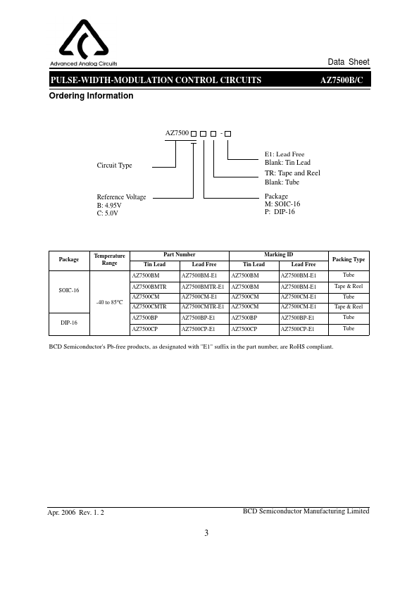
● Internal Circuitry Prohibits Double Pulse at Either control flip-flop, and an output control circuit. The difference between AZ7500B and AZ7500C is that they have 4.95V and 5V reference voltage respectively. The AZ7500B/C is available in standard packages of DIP-16 and SOIC-16.
APPLICATIONS
● SMPS● Back Light Inverter
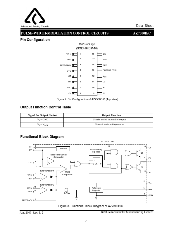
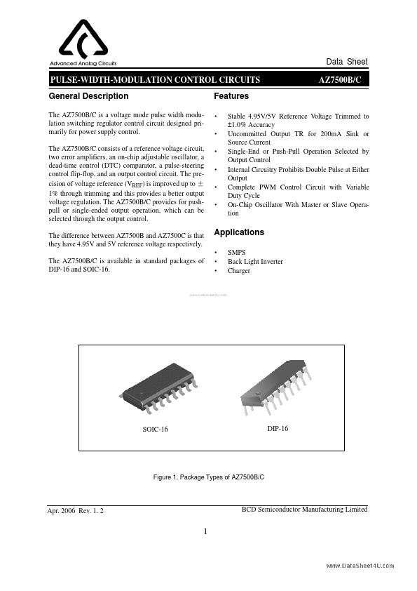
● Charger SOIC-16 DIP-16 Apr. 2006 Rev. 1. 2 Figure 1. Package Types of AZ7500B/C BCD Semiconductor Manufacturing Limited 1 PULSE-WIDTH-MODULATION CONTROL CIRCUITS Pin Configuration 1IN + 1IN FEEDBACK DTC CT RT M/P Package (SOIC-16/DIP-16) 1 16 2 15 3 14 4 13 5 12 6 11 2IN + 2IN REF OUTPUT CTRL VCC C2 GND 7 10 E2 C1 8 9 E1 Figure 2. Pin Configuration...