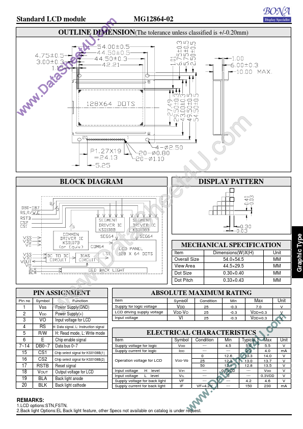
The following content is an automatically extracted verbatim text
from the original manufacturer datasheet and is provided for reference purposes only.
View original datasheet text
Standard LCD module
OUTLINE DIMENSION(The tolerance unless classified is +/-0.20mm)
w
w
a D . w
S a t
e e h
U 4 t
m o .c
MG12864-02
BLOCK DIAGRAM
PIN ASSIGNMENT
Pin no Symbol
1 2 3 4 5 6 7~14 15 16
17 18 19 20
Vss Power Supply(GND) VDD Power Supply(+) VO Input voltage for LCD RS H: Data signal, L: Instruction signal R/W H: Read mode, L: Write mode E Chip enable signal DB0~7 Data bus 0~7 CS1 Chip select signal for KS0108B(1) CS2 Chip select signal for KS0108B(2) RSTB Reset signal VOUT Output voltage for LCD BLA Back light anode BLK Back light cathode
w
Function
w
w
t a .D
Item
MECHANICAL SPECIFICATION
Item Overall Size View Area Dot Size Dot Pitch Dimensions(W)X(H) 54.0×54.5 44.5×29.5 0.30×0.40 0.33×0.