BP2525D
Key Features
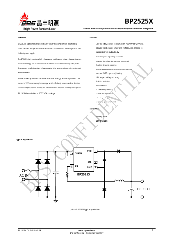
- Overload protection
- Short circuit protection
- Over temperature protection
- Cycle-by-cycle current limit
| Part Number | Manufacturer | Description |
|---|---|---|
| BP252 | Shunye | PRESS-FIT BOSCH DIODES |