BSW6622
Features
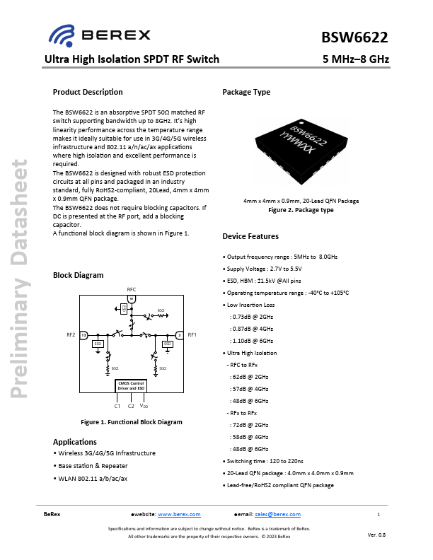
Block Diagram
50Ω
RF2 13
3 RF1
50Ω
50Ω
CMOS Control Driver and ESD
C1 C2 VDD
Figure 1. Func onal Block Diagram
Applica ons
- Wireless 3G/4G/5G Infrastructure
- Base sta on & Repeater
- WLAN 802.11 a/b/ac/ax
- Output frequency range : 5MHz to 8.0GHz
- Supply Voltage : 2.7V to 5.5V
- ESD, HBM : ±1.5k V @All pins
- Opera ng temperature range : -40°C to +105°C
- Low Inser on Loss
: 0.73d B @ 2GHz : 0.87d B @ 4GHz : 1.10d B @ 6GHz
- Ultra High Isola on
- RFC to RFx : 62d B @ 2GHz : 57d B @ 4GHz : 48d B @ 6GHz
- RFx to RFx : 72d B @ 2GHz : 58d B @ 4GHz : 48d B @ 6GHz
- Switching me : 120 to 220ns
- 20-Lead QFN package : 4.0mm x 4.0mm x 0.9mm
- Lead-free/Ro HS2 pliant QFN package
Be Rex
- website: .berex.
- email: sales@berex.
Specifica ons and informa on are subject to change without no ce. Be Rex is a trademark of Be Rex. All other trademarks are the property of their respec ve owners. © 2023 Be Rex
1 Ver. 0.8
Ultra High Isola on SPDT RF Switch
5 MHz- 8...