BeRex BVA3143
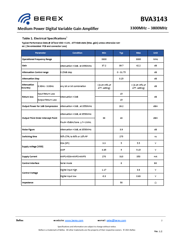
The BVA3143 is a digitally controlled variable gain amplifier (DVGA) in a 6mm x 6mm LGA package, with a frequency range of 3300 to 3800 MHz and an operating VDD of 5.0V. BVA3143 is high performance and high dynamic range makes it ideally suited for use in 5G/LTE wireless infrastructure and other high performance wireless RF applications. The BVA3143 is an integration of a high performance digital 7bit step attenuator (DSA) that provides a 31.75 dB attenuation range in 0.25 dB steps, and high linearity broadband gain block amplifiers featuring high ACP and P1dB.| Part No. | BVA3143 |
|---|---|
| Datasheet | BVA3143 Download |
| Manufacturer |  BeRex |
| Description | Medium Power Digital Variable Gain Amplifier |
| Buy | Stock & Price |
DESCRIPTION
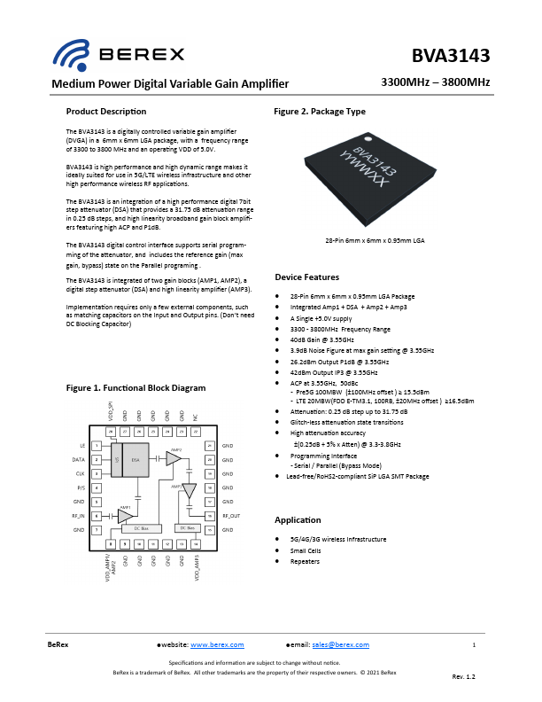
The BVA3143 digital control interface supports serial programming of the attenuator, and includes the reference gain (max gain, bypass) state on the Parallel programing . The BVA3143 is integrated of two gain blocks (AMP1, AMP2), a digital step attenuator (DSA) and high linearity amplifier (AMP3). Implementation requires only a few external components, such as matching capacitors on the Input and Output pins. (Don’t need DC Blocking Capacitor) Figure 1. Functional Block Diagram Figure 2. Package Type 28-Pin 6mm x 6mm x 0.95mm LGA DeviceFEATURES
● 28-Pin 6mm x 6mm x 0.95mm LGA Package● Integrated Amp1 + DSA + Amp2 + Amp3
● A Single +5.0V supply
● 3300 - 3800MHz Frequency Range
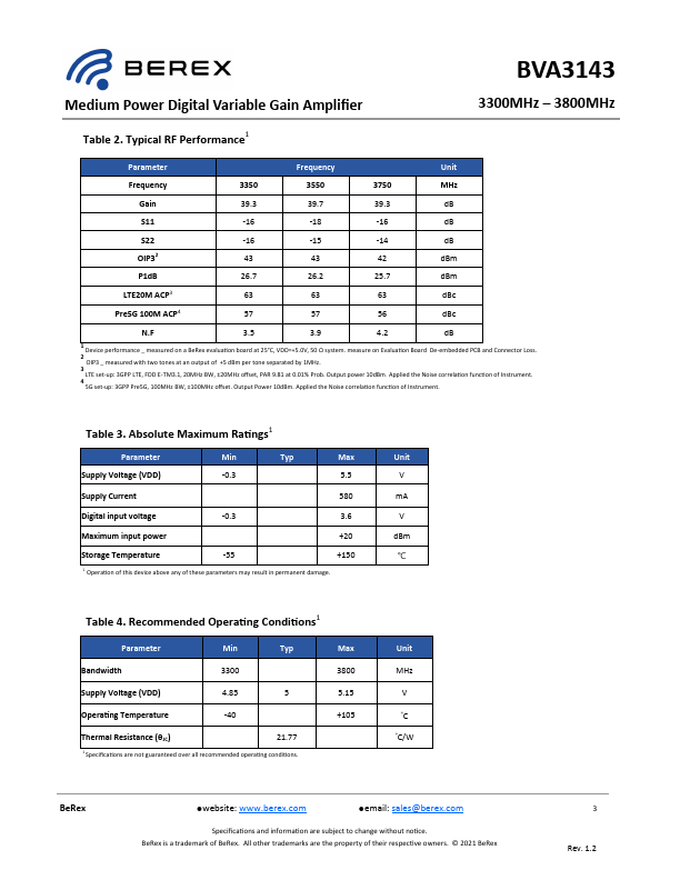
● 40dB Gain @ 3.55GHz
● 3.9dB Noise Figure at max gain setting @ 3.55GHz
● 26.2dBm Output P1dB @ 3.55GHz
● 42dBm Output IP3 @ 3.55GHz
● ACP at 3.55GHz, 50dBc - Pre5G 100MBW (±100MHz offset ) ≥ 15.5dBm - LTE 20MBW(FDD E-TM3.1, 100RB, ±20MHz offset ) ≥16.5dBm
● Attenuation: 0.25 dB step up to 31.75 dB...