BL2004A1 Overview
Description
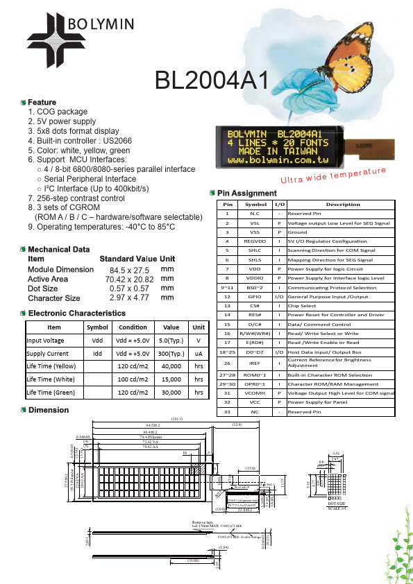
1 N.C - Reserved Pin 2 VSL P Voltage output Low Level for SEG Signal 3 VSS P Ground 4 REGVDD I 5V I/O Regulator ConfiguraƟon 5 SHLC I Scanning DirecƟon for COM Signal 6 SHLS I Mapping DirecƟon for SEG Signal 7 VDD P Power Supply for logic Circuit 8 VDDIO P Power Supply for Interface logic Level 9~11 BS0~2 I CommunicaƟng Protocol SelecƟon 12 GPIO I/O General Purpose Input /Output 13 CS# I Chip Select 14 RES# I Power Reset for Controller and Driver 15 D/C# I Data/ Command Control 16 R/W#(WR#) I Read/ Write Select or Write 17 E(RD#) I Read /Write Enable or Read 18~25 26 D0~D7 IREF I/O Host Data Input/ Output Bus Current Referencefor Brightness I Adjustment 27~28 ROM0~1 I Built-in Character ROM SelecƟon 29~30 OPR0~1 I Character ROM/RAM Management 31 VCOMH P Voltage Output High Level for COM signal 32 VCC P Power Supply for Panel 33 NC - Reserved Pin (32.8) (15.0) 3.55 2.97 0.6 0.57 (7.0) 8 1 0± 0.3 0 .1 ± 0.03 1.8±0.3 3.6±0.2 13.75 5.35 4.77 0.6 0.57 2 7.5±0.2 26.5 Polarizer 22.82 VA 20.82 AA R0.5 W=0.4±0.03 2- 0.8±0.1 1 33 22.0±.