FEATURES
q TWO-CHIP CONSTRUCTION q HIGH-SPEED 16-BIT PARALLEL, 8-BIT (BYTE) PARALLEL, AND SERIAL INPUT MODES q DOUBLE-BUFFERED INPUT REGISTER CONFIGURATION q VOUT AND IOUT MODELS q HIGH ACCURACY: Linearity Error ±0.003% of FSR max Differential Linearity Error ±0.006% of FSR max q MONOTONIC (TO 14 BITS) OVER SPECIFIED TEMPERATURE RANGE q HERMETICALLY SEALED q LOW COST PLASTIC VERSIONS AVAILABLE (DAC707JP/KP) DESCRIPTION
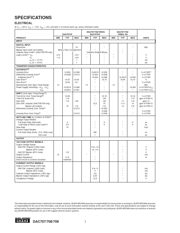
16bit data is loaded in two successive 8-bit bytes into parallel 8-bit latches before being transferred into the D/A latch. Input coding is Binary Two’s Complement (bipolar) or Unipolar Straight Binary (unipolar, when an external logic inverter is used to invert the MSB). In addition, the DAC708/709 can be loaded serially (MSB first). The DAC707 is designed to interface to a 16-bit bus. 8-Bit (DAC708, 709) or 16-Bit (DAC707) Serial Data Low Byte Latch High Byte Latch D/A Latch Reference Circuit 16-Bit D/A Converter Bipolar Offset Data is written into a 16-bit latch and subsequently the D/A latch. Burr-Brown Corporation