ADS5240 Overview
Key Specifications
Pins: 64
Operating Voltage: 3.3 V
Max Voltage (typical range): 3.6 V
Min Voltage (typical range): 3 V
Description
The ADS5240 is a high-performance, 4-channel, 40MSPS analog-to-digital converter (ADC). Internal references are provided, simplifying system design requirements.
Key Features
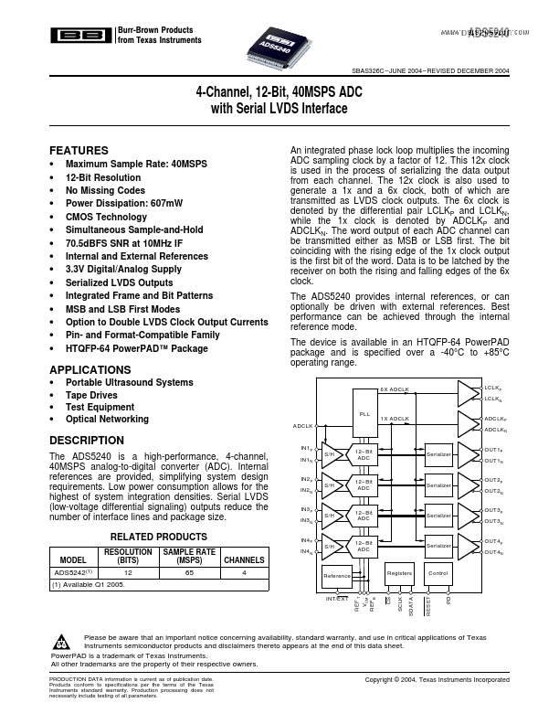
- The 12x clock is also used to generate a 1x and a 6x clock, both of which are transmitted as LVDS clock outputs
- The 6x clock is denoted by the differential pair LCLKP and LCLKN, while the 1x clock is denoted by ADCLKP and ADCLKN
- The word output of each ADC channel can be transmitted either as MSB or LSB first
- The bit coinciding with the rising edge of the 1x clock output is the first bit of the word
- Data is to be latched by the receiver on both the rising and falling edges of the 6x clock
- The ADS5240 provides internal references, or can optionally be driven with external references
- Best performance can be achieved through the internal reference mode
- The device is available in an HTQFP-64 PowerPAD package and is specified over a -40°C to +85°C operating range
- 6X ADCLK LCLK P LCLK N PLL ADCLK ADC LK P ADC LK N