CASS D444
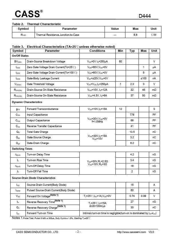
The D444 combines advanced trench MOSFET technology with a low resistance package to provide extremely low RDS(ON).| Part No. | D444 |
|---|---|
| Datasheet | D444 Download |
| Manufacturer | CASS |
| Description | N-Channel Trench Power MOSFET |
| Buy | Stock & Price |
GENERAL DESCRIPTION
Those devices are suitable for use in PWM, load switching and general purpose applications.FEATURES
● VDS=60V; ID=15A RDS(ON)<40mΩ @ VGS=10V● Ultra Low On-Resistance
● High UIS and UIS 100% Test Application
● Power switching application
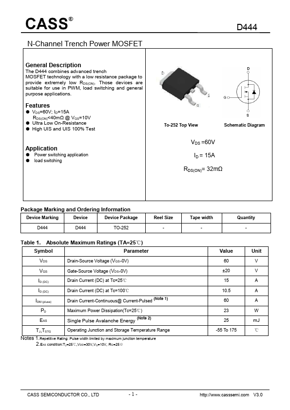
● load switching D444 To-252 Top View Schematic Diagram VDS =60V ID = 15A RDS(ON)= 32mΩ Package Marking and Ordering Information Device Marking Device Device Package D444 D444 TO-252 Reel Size - Table 1.
ABSOLUTE MAXIMUM RATINGS
(TA=25℃) Symbol Parameter VDS Drain-Source Voltage (VGS=0V) VGS Gate-Source Voltage (VDS=0V) ID (DC) ID (DC) IDM (pluse) PD EAS Drain Current (DC) at Tc=25℃ Drain Current (DC) at Tc=100℃ Drain Current-Continuous@ Current-Pulsed (Note 1) Maximum Power Dissipation(Tc=25℃) Single Pulse Avalanche Energy (Note 2) TJ,TSTG Operat