The following content is an automatically extracted verbatim text
from the original manufacturer datasheet and is provided for reference purposes only.
View original datasheet text
Continental Device India Limited
An ISO/TS 16949, ISO 9001 and ISO 14001 Certified Company
BCW29 BCW30
SILICON PLANAR EPITAXIAL TRANSISTORS
P–N–P transistors
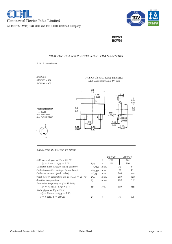
Marking BCW29 = C1 BCW30 = C2
PACKAGE OUTLINE DETAILS ALL DIMENSIONS IN mm
Pin configuration 1 = BASE 2 = EMITTER 3 = COLLECTOR
3
1
2
ABSOLUTE MAXIMUM RATINGS
D.C. current gain at Tj = 25 °C –IC = 2 mA; –VCE = 5 V
Collector–base voltage (open emitter) Collector–emitter voltage (open base) Collector current (peak value) Total power dissipation up to Tamb = 25 °C Junction temperature Transition frequency at f = 35 MHz
–IC = 10 mA; –VCE = 5 V Noise figure at RS = 2 kW
–Ic = 200 mA; –VCE = 5 V; f = 1 kHz; B = 200 Hz
hFE –VCB0 –VCE0 –ICM Ptot Tj
BCW29 > 120 < 260 max. max. max. max, max.