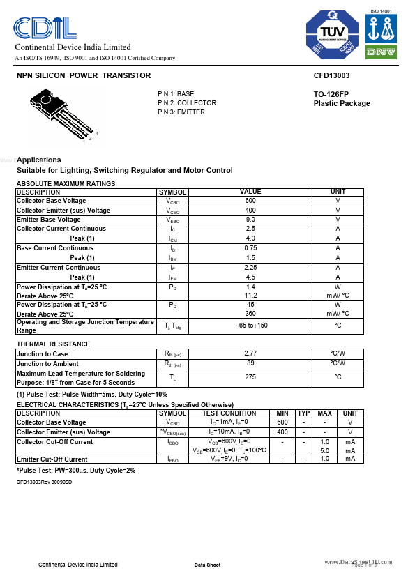
APPLICATIONS
Suitable for Lighting, Switching Regulator and Motor Control ABSOLUTE MAXIMUM RATINGS
DESCRIPTION
Collector Base Voltage Collector Emitter (sus) Voltage Emitter Base Voltage Collector Current Continuous Peak (1) Base Current Continuous Peak (1) Emitter Current Continuous Peak (1) Power Dissipation at Ta=25 ºC Derate Above 25ºC Power Dissipation at Tc=25 ºC Derate Above 25ºC Operating and Storage Junction Temperature Range THERMAL RESISTANCE Junction to Case Junction to Ambient Maximum Lead Temperature for Soldering Purpose: 1/8" from Case for 5 Seconds (1) Pulse Test: Pulse Width=5ms, Duty Cycle=10% ELECTRICAL CHARACTERISTICS
(Ta=25ºC Unless Specified Otherwise) DESCRIPTION
SYMBOL TEST CONDITION VCBO IC=1mA, IE=0 Collector Base Voltage Collector Emitter (sus) Voltage Collector Cut-Off Current Emitter Cut-Off Current *Pulse Test: PW=300µs, Duty Cycle=2% CFD13003Rev 300905D SYMBOL VCBO VCEO VEBO IC ICM IB IBM IE IEM PD PD Tj, Tstg VALUE 600 400 9.0 2.5 4.0 0.75 1.5 2.25 4.5 1.4 11.2 45 360 - 65 to+150 UNIT V V V A A A A A A W mW/ ºC W mW/ ºC ºC Rth (j-c) Rth (j-a) TL 2.77 89 275 ºC/W ºC/W ºC MIN 600 400 - TYP - MAX 1.0 5. Continental Device India