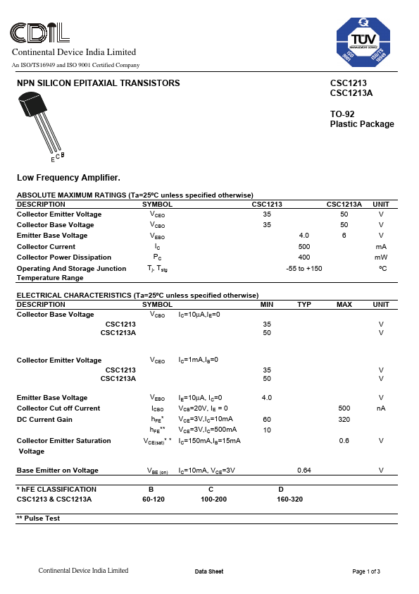
ABSOLUTE MAXIMUM RATINGS
(Ta=25ºC unless specified otherwise) DESCRIPTION
SYMBOL CSC1213 VCEO 35 Collector Emitter Voltage VCBO Collector Base Voltage 35 Emitter Base Voltage Collector Current Collector Power Dissipation Operating And Storage Junction Temperature Range VEBO IC PC Tj, Tstg 4.0 500 400 -55 to +150 CSC1213A 50 50 6 UNIT V V V mA mW ºC ELECTRICAL CHARACTERISTICS
(Ta=25ºC unless specified otherwise) DESCRIPTION
SYMBOL MIN VCBO IC=10µA,IE=0 Collector Base Voltage CSC1213 35 CSC1213A 50 TYP MAX UNIT V V Collector Emitter Voltage CSC1213 CSC1213A Emitter Base Voltage Collector Cut off Current DC Current Gain Collector Emitter Saturation Voltage Base Emitter on Voltage * hFE CLASSIFICATION CSC1213 & CSC1213A ** Pulse Test VCEO IC=1mA,IB=0 35 50 V V V 500 60 10 0.6 V 320 nA VEBO ICBO hFE* hFE** IE=10µA, IC=0 VCB=20V, IE = 0 VCE=3V,IC=10mA VCE=3V,IC=500mA 4.0 VCE(sat)* * IC=150mA,IB=15mA VBE (on) B 60-120 IC=10mA, VCE=3V C 100-200 0.64 D 160-320 V Continental Device India Limited... Continental Device India