ABSOLUTE MAXIMUM RATINGS
DESCRIPTION
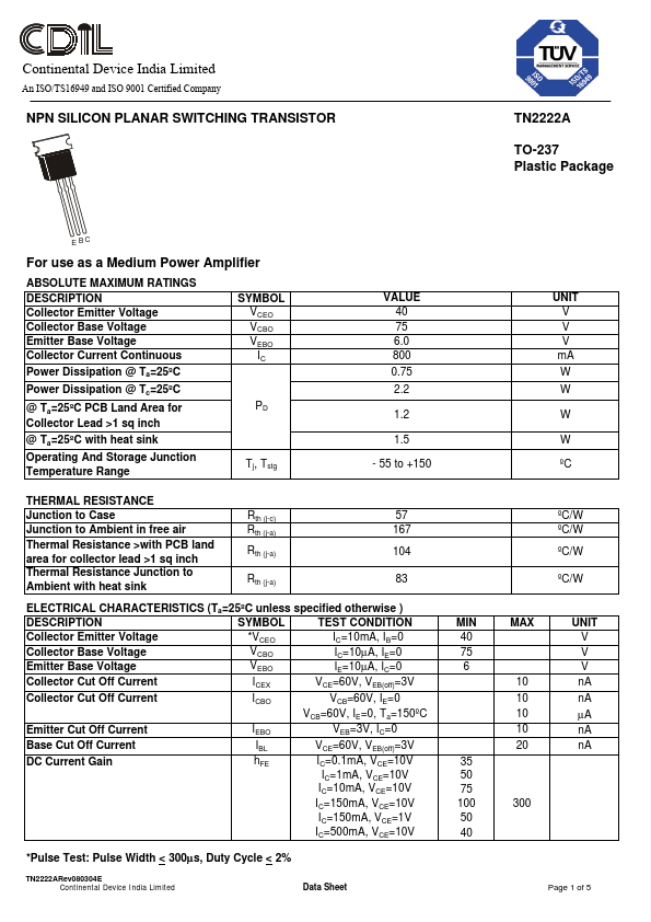
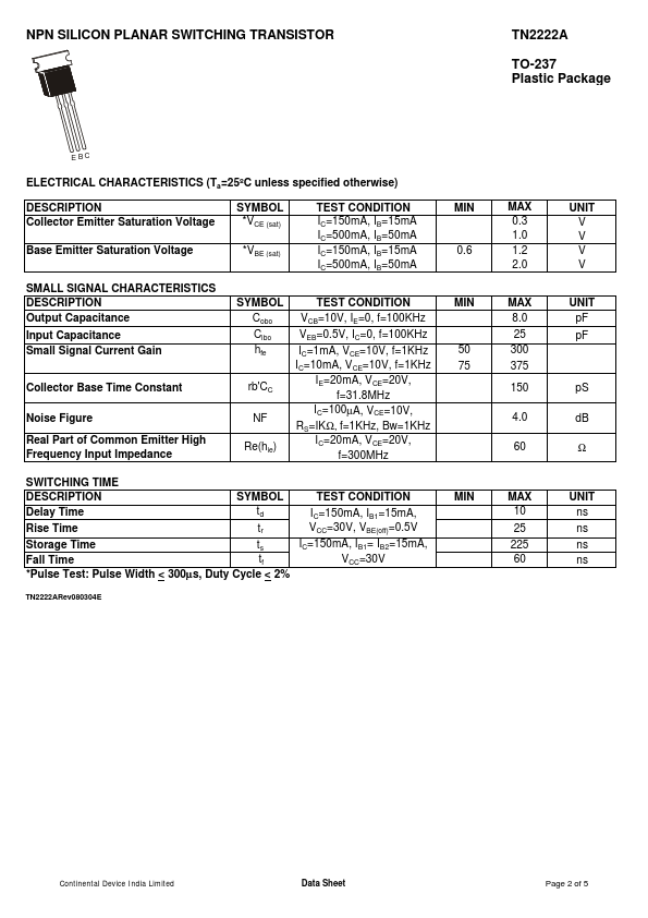
Collector Emitter Voltage Collector Base Voltage Emitter Base Voltage Collector Current Continuous Power Dissipation @ Ta=25ºC Power Dissipation @ Tc=25ºC @ Ta=25ºC PCB Land Area for Collector Lead >1 sq inch @ Ta=25ºC with heat sink Operating And Storage Junction Temperature Range SYMBOL VCEO VCBO VEBO IC PD Tj, Tstg VALUE 40 75 6.0 800 0.75 2.2 1.2 1.5 - 55 to +150 THERMAL RESISTANCE Junction to Case Junction to Ambient in free air Thermal Resistance >with PCB land area for collector lead >1 sq inch Thermal Resistance Junction to Ambient with heat sink Rth (j-c) Rth (j-a) Rth (j-a) Rth (j-a) 57 167 104 83 ELECTRICAL CHARACTERISTICS
(Ta=25ºC unless specified otherwise ) DESCRIPTION
SYMBOL TEST CONDITION Collector Emitter Voltage *VCEO IC=10mA, IB=0 Collector Base Voltage Emitter Base Voltage VCBO VEBO IC=10µA, IE=0 IE=10µA, IC=0 Collector Cut Off Current ICEX VCE=60V, VEB(off)=3V Collector Cut Off Current ICBO VCB=60V, IE=0 VCB=60V, IE=0, Ta=150ºC... Continental Device India