Datasheet4U Logo Datasheet4U.com

CEB20P10 - P-Channel Enhancement Mode Field Effect Transistor

Datasheet Summary

Features

  • -100V, -20A, RDS(ON) =130mΩ @VGS = -10V. Super high dense cell design for extremely low RDS(ON). High power and current handing capability. Lead-free plating ; RoHS compliant. TO-220 & TO-263 package. D D G S CEB SERIES TO-263(DD-PAK) G D S CEP SERIES TO-220 G S.

📥 Download Datasheet

Datasheet preview – CEB20P10

Datasheet Details

Part number CEB20P10
Manufacturer CET
File Size 372.75 KB
Description P-Channel Enhancement Mode Field Effect Transistor
Datasheet download datasheet CEB20P10 Datasheet
Additional preview pages of the CEB20P10 datasheet.
Other Datasheets by CET

Full PDF Text Transcription

Click to expand full text
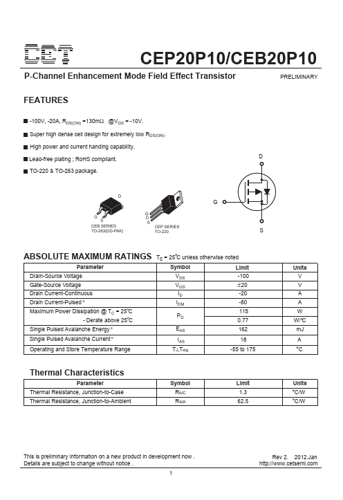
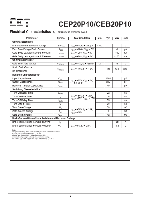
CEP20P10/CEB20P10 P-Channel Enhancement Mode Field Effect Transistor PRELIMINARY FEATURES -100V, -20A, RDS(ON) =130mΩ @VGS = -10V. Super high dense cell design for extremely low RDS(ON). High power and current handing capability. Lead-free plating ; RoHS compliant. TO-220 & TO-263 package. D D G S CEB SERIES TO-263(DD-PAK) G D S CEP SERIES TO-220 G S ABSOLUTE MAXIMUM RATINGS Tc = 25 C unless otherwise noted Parameter Symbol Limit Drain-Source Voltage Gate-Source Voltage Drain Current-Continuous Drain Current-Pulsed a Maximum Power Dissipation @ TC = 25 C - Derate above 25 C VDS VGS ID IDM PD -100 ±20 -20 -80 115 0.
Published: |